JAJSHV5B June 2017 – August 2019 ADS1287
PRODUCTION DATA.
- 1 特長
- 2 アプリケーション
- 3 概要
- 4 改訂履歴
- 5 概要(続き)
- 6 Pin Configuration and Functions
- 7 Specifications
- 8 Parameter Measurement Information
-
9 Detailed Description
- 9.1 Overview
- 9.2 Functional Block Diagram
- 9.3 Feature Description
- 9.4 Device Functional Modes
- 9.5
Programming
- 9.5.1 Serial Interface
- 9.5.2
Commands
- 9.5.2.1 WAKEUP: Wake Up Command
- 9.5.2.2 STANDBY: Standby Mode Command
- 9.5.2.3 SYNC: Synchronize ADC Conversions
- 9.5.2.4 RESET: Reset Command
- 9.5.2.5 RDATAC: Read Data Continuous Mode Command
- 9.5.2.6 SDATAC: Stop Read Data Continuous Mode Command
- 9.5.2.7 RDATA: Read Data Command
- 9.5.2.8 RREG: Read Register Data Command
- 9.5.2.9 WREG: Write Register Data Command
- 9.5.2.10 OFSCAL: Offset Calibration Command
- 9.5.2.11 GANCAL: Gain Calibration Command
- 9.6
Register Map
- 9.6.1
Register Descriptions
- 9.6.1.1 ID/CFG: ID, Configuration Register (address = 00h) [reset = x0h]
- 9.6.1.2 CONFIG0: Configuration Register 0 (address = 01h) [reset = 52h]
- 9.6.1.3 CONFIG1: Configuration Register 1 (address = 02h) [reset = 08h]
- 9.6.1.4 High-Pass Filter Corner Frequency (HPFx) Registers (address = 03h, 04h) [reset = 32h, 03h]
- 9.6.1.5 Offset Calibration (OFCx) Registers (address = 05h, 06h, 07h) [reset = 00h, 00h, 00h]
- 9.6.1.6 Full-Scale Calibration (FSCx) Registers (address = 08h, 09h, 0Ah) [reset = 00h, 00h, 40h]
- 9.6.1
Register Descriptions
- 10Application and Implementation
- 11Power Supply Recommendations
- 12Layout
- 13デバイスおよびドキュメントのサポート
- 14メカニカル、パッケージ、および注文情報
パッケージ・オプション
デバイスごとのパッケージ図は、PDF版データシートをご参照ください。
メカニカル・データ(パッケージ|ピン)
- RHF|24
サーマルパッド・メカニカル・データ
発注情報
9.3.4 Voltage Reference Inputs (REFP, REFN)
The ADC requires an external reference voltage for operation. The specified reference voltage is 2.5 V and is defined by Equation 6 as the voltage between the REFP and REFN pins:
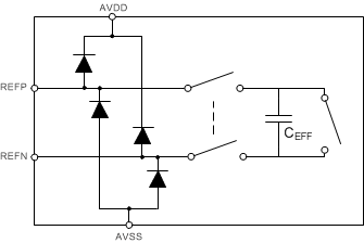
Figure 47 shows the reference input circuit. The ADC samples the reference voltage to an internal capacitor. The sampled voltage is used in the ADC process. The constant sampling of the reference inputs results in transient currents that must be filtered by an external capacitor. Place a 0.1-µF ceramic capacitor directly between the REFP and REFN pins to filter the transient currents.
The input impedance of the reference input is determined by the average value of the transient currents. In applications where one voltage reference drives multiple ADCs, use individual capacitors at each ADC reference input. Reference voltage noise can degrade the overall noise performance. Therefore, the selection of the voltage reference must include the evaluation of noise.
 Figure 47. Simplified Reference Input Circuit
 The ADC reference inputs are protected by internal ESD diodes. The voltage of reference inputs must stay within the range shown in Equation 7 in order to prevent these diodes from conducting:
If the voltage on the reference inputs exceeds this range, limit the reference input current to 10 mA or less. See the Electrical Characteristics section for the specified reference voltage range.