JAJSHV5B June 2017 – August 2019 ADS1287
PRODUCTION DATA.
- 1 特長
- 2 アプリケーション
- 3 概要
- 4 改訂履歴
- 5 概要(続き)
- 6 Pin Configuration and Functions
- 7 Specifications
- 8 Parameter Measurement Information
-
9 Detailed Description
- 9.1 Overview
- 9.2 Functional Block Diagram
- 9.3 Feature Description
- 9.4 Device Functional Modes
- 9.5
Programming
- 9.5.1 Serial Interface
- 9.5.2
Commands
- 9.5.2.1 WAKEUP: Wake Up Command
- 9.5.2.2 STANDBY: Standby Mode Command
- 9.5.2.3 SYNC: Synchronize ADC Conversions
- 9.5.2.4 RESET: Reset Command
- 9.5.2.5 RDATAC: Read Data Continuous Mode Command
- 9.5.2.6 SDATAC: Stop Read Data Continuous Mode Command
- 9.5.2.7 RDATA: Read Data Command
- 9.5.2.8 RREG: Read Register Data Command
- 9.5.2.9 WREG: Write Register Data Command
- 9.5.2.10 OFSCAL: Offset Calibration Command
- 9.5.2.11 GANCAL: Gain Calibration Command
- 9.6
Register Map
- 9.6.1
Register Descriptions
- 9.6.1.1 ID/CFG: ID, Configuration Register (address = 00h) [reset = x0h]
- 9.6.1.2 CONFIG0: Configuration Register 0 (address = 01h) [reset = 52h]
- 9.6.1.3 CONFIG1: Configuration Register 1 (address = 02h) [reset = 08h]
- 9.6.1.4 High-Pass Filter Corner Frequency (HPFx) Registers (address = 03h, 04h) [reset = 32h, 03h]
- 9.6.1.5 Offset Calibration (OFCx) Registers (address = 05h, 06h, 07h) [reset = 00h, 00h, 00h]
- 9.6.1.6 Full-Scale Calibration (FSCx) Registers (address = 08h, 09h, 0Ah) [reset = 00h, 00h, 40h]
- 9.6.1
Register Descriptions
- 10Application and Implementation
- 11Power Supply Recommendations
- 12Layout
- 13デバイスおよびドキュメントのサポート
- 14メカニカル、パッケージ、および注文情報
パッケージ・オプション
デバイスごとのパッケージ図は、PDF版データシートをご参照ください。
メカニカル・データ(パッケージ|ピン)
- RHF|24
サーマルパッド・メカニカル・データ
発注情報
9.3.5.2 FIR Filter Stage
The second stage of the ADS1287 digital filter is the FIR low-pass filter. Data are supplied to the FIR stage from the pre-filter, sinc stage. The FIR filter performs the final frequency response shaping. Figure 51 shows that the FIR filter is composed of four sub-stages.
 Figure 51. FIR Filter
 The first two FIR stages are half-band filters with fixed decimation ratios equal to 2. The third stage decimates by a ratio equal to 4, and the fourth stage decimates by ratio equal to 2. The overall decimation ratio of the FIR stage is 32. Two coefficient sets are selectable by register bits for the third and fourth sections, one for the linear phase and one for the minimum phase response. Table 9 lists the data rates and combined decimation ratios of the sinc and FIR stage. Table 10 lists the filter coefficients that correspond to each FIR stage.
Table 9. FIR Filter Data Rates
Table 10. FIR Stage Coefficients
| COEFFICIENT | SECTION 1 | SECTION 2 | SECTION 3 | SECTION 4 | ||
|---|---|---|---|---|---|---|
| LINEAR PHASE
SCALING = 1 / 512 |
LINEAR PHASE
SCALING = 1 / 8388608 |
SCALING = 1 / 134217728 | SCALING = 1 / 134217728 | |||
| LINEAR
PHASE |
MINIMUM
PHASE |
LINEAR
PHASE |
MINIMUM
PHASE |
|||
| b0 | 3 | –10944 | 0 | 819 | –132 | 11767 |
| b1 | 0 | 0 | 0 | 8211 | –432 | 133882 |
| b2 | –25 | 103807 | –73 | 44880 | –75 | 769961 |
| b3 | 0 | 0 | –874 | 174712 | 2481 | 2940447 |
| b4 | 150 | –507903 | –4648 | 536821 | 6692 | 8262605 |
| b5 | 256 | 0 | –16147 | 1372637 | 7419 | 17902757 |
| b6 | 150 | 2512192 | –41280 | 3012996 | –266 | 30428735 |
| b7 | 0 | 4194304 | –80934 | 5788605 | –10663 | 40215494 |
| b8 | –25 | 2512192 | –120064 | 9852286 | –8280 | 39260213 |
| b9 | 0 | 0 | –118690 | 14957445 | 10620 | 23325925 |
| b10 | 3 | –507903 | –18203 | 20301435 | 22008 | –1757787 |
| b11 | 0 | 224751 | 24569234 | 348 | –21028126 | |
| b12 | 103807 | 580196 | 26260385 | –34123 | –21293602 | |
| b13 | 0 | 893263 | 24247577 | –25549 | –3886901 | |
| b14 | –10944 | 891396 | 18356231 | 33460 | 14396783 | |
| b15 | 293598 | 9668991 | 61387 | 16314388 | ||
| b16 | –987253 | 327749 | –7546 | 1518875 | ||
| b17 | –2635779 | –7171917 | –94192 | –12979500 | ||
| b18 | –3860322 | –10926627 | –50629 | –11506007 | ||
| b19 | –3572512 | –10379094 | 101135 | 2769794 | ||
| b20 | –822573 | –6505618 | 134826 | 12195551 | ||
| b21 | 4669054 | –1333678 | –56626 | 6103823 | ||
| b22 | 12153698 | 2972773 | –220104 | –6709466 | ||
| b23 | 19911100 | 5006366 | –56082 | –9882714 | ||
| b24 | 25779390 | 4566808 | 263758 | –353347 | ||
| b25 | 27966862 | 2505652 | 231231 | 8629331 | ||
| b26 | 25779390 | 126331 | –215231 | 5597927 | ||
| b27 | 19911100 | –1496514 | –430178 | –4389168 | ||
| b28 | 12153698 | –1933830 | 34715 | –7594158 | ||
| b29 | 4669054 | –1410695 | 580424 | –428064 | ||
| b30 | –822573 | –502731 | 283878 | 6566217 | ||
| b31 | –3572512 | 245330 | –588382 | 4024593 | ||
| b32 | –3860322 | 565174 | –693209 | –3679749 | ||
| b33 | –2635779 | 492084 | 366118 | –5572954 | ||
| b34 | –987253 | 231656 | 1084786 | 332589 | ||
| b35 | 293598 | –9196 | 132893 | 5136333 | ||
| b36 | 891396 | –125456 | –1300087 | 2351253 | ||
| b37 | 893263 | –122207 | –878642 | –3357202 | ||
| b38 | 580196 | –61813 | 1162189 | –3767666 | ||
| b39 | 224751 | –4445 | 1741565 | 1087392 | ||
| b40 | –18203 | 22484 | –522533 | 3847821 | ||
| b41 | –118690 | 22245 | –2490395 | 919792 | ||
| b42 | –120064 | 10775 | –688945 | –2918303 | ||
| b43 | –80934 | 940 | 2811738 | –2193542 | ||
| b44 | –41280 | –2953 | 2425494 | 1493873 | ||
| b45 | –16147 | –2599 | –2338095 | 2595051 | ||
| b46 | –4648 | –1052 | –4511116 | –79991 | ||
| b47 | –874 | –43 | 641555 | –2260106 | ||
| b48 | –73 | 214 | 6661730 | –963855 | ||
| b49 | 0 | 132 | 2950811 | 1482337 | ||
| b50 | 0 | 33 | –8538057 | 1480417 | ||
| b51 | 0 | 0 | –10537298 | –586408 | ||
| b52 | 9818477 | –1497356 | ||||
| b53 | 41426374 | –168417 | ||||
| b54 | 56835776 | 1166800 | ||||
| b55 | 41426374 | 644405 | ||||
| b56 | 9818477 | –675082 | ||||
| b57 | –10537298 | –806095 | ||||
| b58 | –8538057 | 211391 | ||||
| b59 | 2950811 | 740896 | ||||
| b60 | 6661730 | 141976 | ||||
| b61 | 641555 | –527673 | ||||
| b62 | –4511116 | –327618 | ||||
| b63 | –2338095 | 278227 | ||||
| b64 | 2425494 | 363809 | ||||
| b65 | 2811738 | –70646 | ||||
| b66 | –688945 | –304819 | ||||
| b67 | –2490395 | –63159 | ||||
| b68 | –522533 | 205798 | ||||
| b69 | 1741565 | 124363 | ||||
| b70 | 1162189 | –107173 | ||||
| b71 | –878642 | –131357 | ||||
| b72 | –1300087 | 31104 | ||||
| b73 | 132893 | 107182 | ||||
| b74 | 1084786 | 15644 | ||||
| b75 | 366118 | –71728 | ||||
| b76 | –693209 | –36319 | ||||
| b77 | –588382 | 38331 | ||||
| b78 | 283878 | 38783 | ||||
| b79 | 580424 | –13557 | ||||
| b80 | 34715 | –31453 | ||||
| b81 | –430178 | –1230 | ||||
| b82 | –215231 | 20983 | ||||
| b83 | 231231 | 7729 | ||||
| b84 | 263758 | –11463 | ||||
| b85 | –56082 | –8791 | ||||
| b86 | –220104 | 4659 | ||||
| b87 | –56626 | 7126 | ||||
| b88 | 134826 | –732 | ||||
| b89 | 101135 | –4687 | ||||
| b90 | –50629 | –976 | ||||
| b91 | –94192 | 2551 | ||||
| b92 | –7546 | 1339 | ||||
| b93 | 61387 | –1103 | ||||
| b94 | 33460 | –1085 | ||||
| b95 | –25549 | 314 | ||||
| b96 | –34123 | 681 | ||||
| b97 | 348 | 16 | ||||
| b98 | 22008 | –349 | ||||
| b99 | 10620 | –96 | ||||
| b100 | –8280 | 144 | ||||
| b101 | –10663 | 78 | ||||
| b102 | –266 | –46 | ||||
| b103 | 7419 | –42 | ||||
| b104 | 6692 | 9 | ||||
| b105 | 2481 | 16 | ||||
| b106 | –75 | 0 | ||||
| b107 | –432 | –4 | ||||
| b108 | –132 | 0 | ||||
| b109 | 0 | 0 | ||||
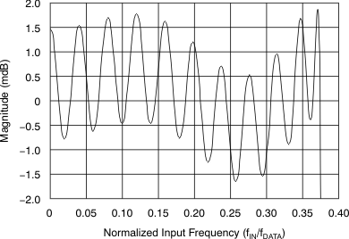
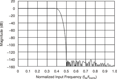
As shown in Figure 52, the FIR frequency response provides a flat pass-band response (±0.003 dB) to 0.375 fDATA. Figure 53 shows the transition band beginning from the edge of the pass band and ending at the beginning of the stop band. The stop-band response is typically –135 dB above the Nyquist frequency.
As with all oversampled systems, the pass-band response repeats at the underlying ADC sample rate. In this case, the response repeats at multiples of the modulator frequency (N·fMOD – f0 and N·fMOD + f0, where N = 1, 2, and so on, and f0 = filter pass band). These image frequencies, if not filtered and otherwise present in the signal, fold back (or alias) into the pass band causing errors. A low-pass input filter reduces aliasing. For many applications, the single-pole filter provided at the PGA output is sufficient to suppress the aliased frequencies.
 Figure 52. FIR Filter Pass-Band Magnitude Response
  Figure 53. FIR Filter Transition Band Magnitude Response