JAJSEU9B September 2017 – September 2019 BQ25910
PRODUCTION DATA.
- 1 特長
- 2 アプリケーション
- 3 概要
- 4 改訂履歴
- 5 Pin Configuration and Functions
- 6 Specifications
-
7 Detailed Description
- 7.1 Overview
- 7.2 Functional Block Diagram
- 7.3
Feature Description
- 7.3.1 Device Power-On-Reset (POR)
- 7.3.2 Device Power Up from Battery without Input Source
- 7.3.3 Device Power Up from Input Source
- 7.3.4 Power Up REGN LDO
- 7.3.5 Poor Source Qualification
- 7.3.6 Converter Power-Up
- 7.3.7 Three-Level Buck Converter Theory of Operation
- 7.3.8 Host Mode and Default Mode
- 7.3.9 Battery Charging Management
- 7.3.10 Master Charger and Parallel Charger Interactions
- 7.3.11 Battery Charging Profile
- 7.4 Device Functional Modes
- 7.5 Programming
- 7.6
Register Maps
- 7.6.1
I2C Registers
- 7.6.1.1 Battery Voltage Regulation Limit Register (Address = 0h) [reset = AAh]
- 7.6.1.2 Charger Current Limit Register (Address = 1h) [reset = 46h]
- 7.6.1.3 Input Voltage Limit Register (Address = 2h) [reset = 04h]
- 7.6.1.4 Input Current Limit Register (Address = 3h) [reset = 13h]
- 7.6.1.5 Reserved Register (Address = 4h) [reset = 03h]
- 7.6.1.6 Charger Control 1 Register (Address = 5h) [reset = 9Dh]
- 7.6.1.7 Charger Control 2 Register (Address = 6h) [reset = 33h]
- 7.6.1.8 INT Status Register (Address = 7h) [reset = X]
- 7.6.1.9 FAULT Status Register (Address = 8h) [reset = X]
- 7.6.1.10 INT Flag Status Register (Address = 9h) [reset = 00h]
- 7.6.1.11 FAULT Flag Register (Address = Ah) [reset = 00h]
- 7.6.1.12 INT Mask Register (Address = Bh) [reset = 00h]
- 7.6.1.13 FAULT Mask Register (Address = Ch) [reset = 00h]
- 7.6.1.14 Part Information Register (Address = Dh) [reset = 0Ah]
- 7.6.1
I2C Registers
- 8 Application and Implementation
- 9 Power Supply Recommendations
- 10Layout
- 11デバイスおよびドキュメントのサポート
- 12メカニカル、パッケージ、および注文情報
パッケージ・オプション
デバイスごとのパッケージ図は、PDF版データシートをご参照ください。
メカニカル・データ(パッケージ|ピン)
- YFF|36
サーマルパッド・メカニカル・データ
発注情報
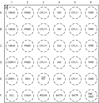
5 Pin Configuration and Functions
BQ25910-YFF (I2C controlled)
36-Pin DSBGA
Top View

1. Top View = Xray through a soldered down part with A1 starting in upper left hand corner.
Pin Functions
| PIN | I/O | DESCRIPTION | |
|---|---|---|---|
| NAME | NO. | ||
| BATN | F4 | AI | Negative Battery Sense Terminal – Kelvin connect via 100-Ω resistor as close as possible to negative battery terminal |
| BATP | F5 | AI | Positive Battery Sense Terminal – Kelvin connect via 100-Ω resistor as close as possible to positive battery terminal |
| CAUX | F2 | P | Auxiliary Capacitor – Bypass CAUX to GND with at least a 4.7-μF, 10-V ceramic capacitor |
| CDRV+ | D1 | P | Gate Drive Supply Positive Terminal – CDRV is used to generate multilevel gate drive rails.
Connect a 220-nF, 6.3-V ceramic capacitor across CDRV+ and CDRV-. |
| CDRV– | E1 | P | Gate Drive Supply Negative Terminal – CDRV is used to generate multilevel gate drive rails.
Connect a 220-nF, 6.3-V ceramic capacitor across DRV+ and DRV-. |
| CFLY+ | A3 | P | Flying Capacitor Positive Terminal – Connect 20-μF, 16-V ceramic capacitor across CFLY+ and CFLY–. Refer to Application and Implementation section for more information on selecting CFLY. |
| B3 | |||
| C3 | |||
| D3 | |||
| CFLY– | A5 | P | Flying Capacitor Negative Terminal – Connect 20-μF, 16-V ceramic capacitor across CFLY+ and CFLY–. Refer to Application and Implementation section for more information on selecting CFLY. |
| B5 | |||
| C5 | |||
| D5 | |||
| E5 | |||
| GND | A6 | - | Ground Return |
| B6 | |||
| C6 | |||
| D6 | |||
| E6 | |||
| IND_SNS | F6 | AI | Output Inductor Sense Input – Kelvin connect as close as possible to the output of the switched inductor. |
| INT | E3 | DO | Open-Drain Interrupt Output – Connect INT to the logic rail via a 10-kΩ resistor. The INT pin sends active low, 256-μs pulse to the host to report charger device status and fault. |
| PMID | A2 | P | Reverse Blocking MOSFET and QHSA MOSFET Connection – Given the total input capacitance, place 1 μF on VBUS, and the rest on PMID, as close to the device as possible. Typical value: 10-μF, 25-V ceramic capacitor |
| B2 | |||
| C2 | |||
| D2 | |||
| REGN | F3 | P | Gate Drive Supply – Bias supply for internal MOSFETs driver and device. Bypass REGN to GND with a 4.7-μF, 10-V ceramic capacitor. |
| SCL | F1 | DI | I2C Interface Open-Drain Clock Line – Connect SCL to the logic rail through a 10-kΩ resistor. |
| SDA | E2 | DIO | I2C Interface Open-Drain Data Line – Connect SDA to the logic rail through a 10-kΩ resistor. |
| SW | A4 | P | Inductor Connection – Connect to the switched side of the external inductor (Recommended: 330 nH for up to 9-V applications or 470 nH for up to 12-V applications). Refer to Application and Implementation section for more information on selecting inductor. |
| B4 | |||
| C4 | |||
| D4 | |||
| E4 | |||
| VBUS | A1 | P | Input Supply – VBUS is connected to the external DC supply. Bypass VBUS to GND with at least 1-μF, 25-V ceramic capacitor, placed as close to the device as possible. |
| B1 | |||
| C1 | |||