JAJSG82A November 2015 – September 2018
PRODUCTION DATA.
- 1 特長
- 2 アプリケーション
- 3 概要
- 4 改訂履歴
- 5 Pin Configuration and Functions
- 6 Specifications
- 7 Detailed Description
- 8 Application and Implementation
- 9 Power Supply Recommendations
- 10Layout
- 11デバイスおよびドキュメントのサポート
- 12メカニカル、パッケージ、および注文情報
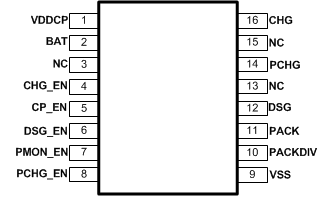
5 Pin Configuration and Functions
PW Package
16-pin TSSOP
Top View

Pin Functions
| PIN | TYPE(1) | DESCRIPTION | |
|---|---|---|---|
| NAME | NO. | I/O | |
| BAT | 2 | P | Top of battery stack |
| CHG(2) | 16 | O | Gate drive for charge FET |
| CHG_EN(3) | 4 | I | Charge FET enable |
| CP_EN(3) | 5 | I | Charge pump enable (internally logic OR'ed with CHG_EN and DSG_EN signals) |
| DSG(2) | 12 | O | Gate drive for discharge FET |
| DSG_EN(3) | 6 | I | Discharge FET enable |
| NC | 3, 13, 15 | — | No connect. Leave the pin floating |
| PACK | 11 | P | Analog input from PACK+ terminal |
| PACKDIV(2) | 10 | O | PACK voltage after internal switch (Connect to MCU ADC via resistor divider.) |
| PCHG(2) | 14 | O | Gate drive for pre-charge FET |
| PCHG_EN(3) | 8 | I | Pre-charge FET enable |
| PMON_EN(3) | 7 | I | Pack monitor enable (allows connection of internal switch between PACK and PACKDIV) |
| VDDCP | 1 | O | Charge pump output. Connect a capacitor to BAT pin. Do not load this pin. |
| VSS | 9 | P | Ground reference |
(1) P = Power Connection, O = Digital Output, AI = Analog Input, I = Digital Input, I/OD = Digital Input/Output
(2) Leave the pin float if function is not used.
(3) Recommended to connect the pin to ground if function is not used.