JAJSF40 March 2018 CSD86356Q5D
PRODUCTION DATA.
- 1特長
- 2アプリケーション
- 3概要
- 4改訂履歴
-
5Specifications
- 5.1 Absolute Maximum Ratings
- 5.2 Recommended Operating Conditions
- 5.3 Thermal Information
- 5.4 Power Block Performance
- 5.5 Electrical Characteristics – Q1 Control FET
- 5.6 Electrical Characteristics – Q2 Sync FET
- 5.7 Typical Power Block Device Characteristics
- 5.8 Typical Power Block MOSFET Characteristics
- 6Application and Implementation
- 7Layout
- 8デバイスおよびドキュメントのサポート
- 9メカニカル、パッケージ、および注文情報
7.1 Recommended Schematic Overview
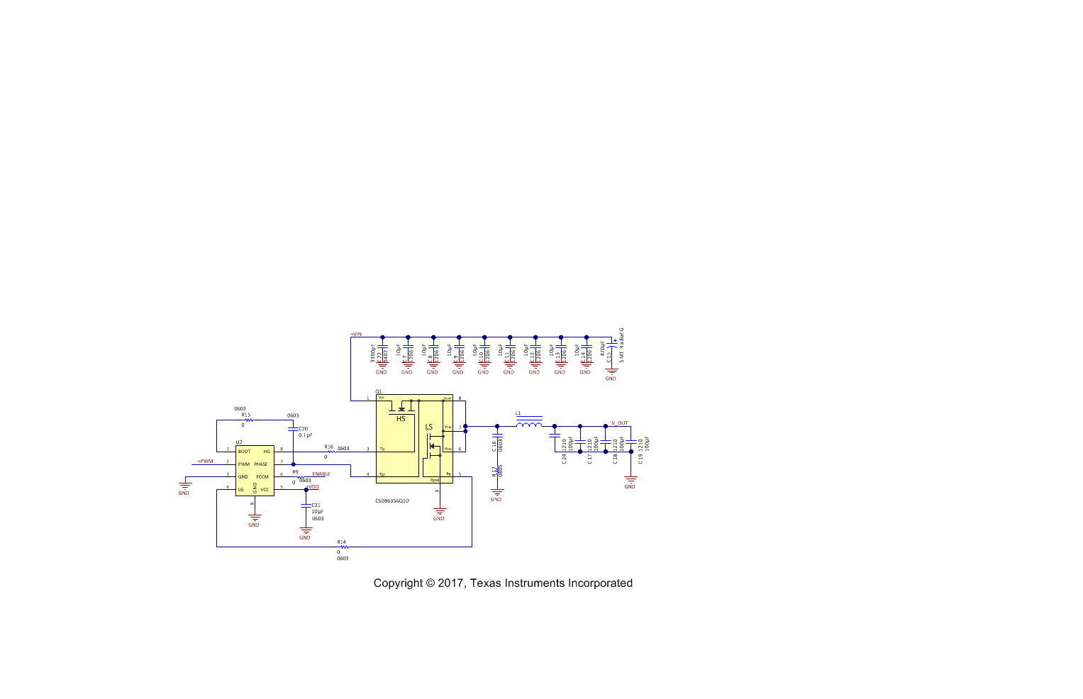
There are several critical components that must be used in conjunction with this power block device. Figure 32 shows a portion of a schematic with the critical components needed for proper operation.
- C22: Bypass capacitor for VIN to help with ringing reduction (recommend 3.3-nF, 0402, 50-V ceramic capacitor)
- C20: Bootstrap capacitor
- C21: Bypass capacitor for VDD
- C7-C14: Bypass capacitors for VIN (minimum of 40 µF)
- C15: Electrolytic capacitor for VIN
- R14, R16: Place holder for gate resistor (optional)
- R15: Place holder for bootstrap resistor (optional)
- R17, C16: Place holder for snubber (optional)
 Figure 32. Recommended Schematic