JAJSB09K January   2010  – February 2018 LM27402

PRODUCTION DATA.  

  1. 特長
  2. アプリケーション
  3. 概要
    1.     Device Images
      1.      代表的なアプリケーション回路
  4. 改訂履歴
  5. Pin Configuration and Functions
    1.     Pin Functions
  6. Specifications
    1. 6.1 Absolute Maximum Ratings
    2. 6.2 ESD Ratings
    3. 6.3 Recommended Operating Conditions
    4. 6.4 Thermal Information
    5. 6.5 Electrical Characteristics
    6. 6.6 Timing Requirements
    7. 6.7 Switching Characteristics
    8. 6.8 Typical Performance Characteristics
  7. Detailed Description
    1. 7.1 Overview
    2. 7.2 Functional Block Diagram
    3. 7.3 Feature Description
      1. 7.3.1  Wide Input Voltage Range
      2. 7.3.2  UVLO
      3. 7.3.3  Precision Enable
      4. 7.3.4  Soft-Start and Voltage Tracking
      5. 7.3.5  Output Voltage Setpoint and Accuracy
      6. 7.3.6  Voltage-Mode Control
      7. 7.3.7  Power Good
      8. 7.3.8  Inductor-DCR-Based Overcurrent Protection
      9. 7.3.9  Current Sensing
      10. 7.3.10 Power MOSFET Gate Drivers
      11. 7.3.11 Pre-Bias Start-up
    4. 7.4 Device Functional Modes
      1. 7.4.1 Fault Conditions
        1. 7.4.1.1 Thermal Protection
        2. 7.4.1.2 Current Limit
        3. 7.4.1.3 Negative Current Limit
        4. 7.4.1.4 Undervoltage Threshold (UVT)
        5. 7.4.1.5 Overvoltage Threshold (OVT)
  8. Application and Implementation
    1. 8.1 Application Information
      1. 8.1.1  Converter Design
      2. 8.1.2  Inductor Selection (L)
      3. 8.1.3  Output Capacitor Selection (COUT)
      4. 8.1.4  Input Capacitor Selection (CIN)
      5. 8.1.5  Using Precision Enable
      6. 8.1.6  Setting the Soft-Start Time
      7. 8.1.7  Tracking
      8. 8.1.8  Setting the Switching Frequency
      9. 8.1.9  Setting the Current Limit Threshold
      10. 8.1.10 Control Loop Compensation
      11. 8.1.11 MOSFET Gate Drivers
      12. 8.1.12 Power Loss and Efficiency Calculations
        1. 8.1.12.1 Power MOSFETs
        2. 8.1.12.2 High-Side Power MOSFET
        3. 8.1.12.3 Low-Side Power MOSFET
        4. 8.1.12.4 Gate-Charge Loss
        5. 8.1.12.5 Input and Output Capacitor ESR Losses
        6. 8.1.12.6 Inductor Losses
        7. 8.1.12.7 Controller Losses
        8. 8.1.12.8 Overall Efficiency
    2. 8.2 Typical Applications
      1. 8.2.1 Example Circuit 1
        1. 8.2.1.1 Design Requirements
        2. 8.2.1.2 Detailed Design Procedure
          1. 8.2.1.2.1 Custom Design With WEBENCH® Tools
        3. 8.2.1.3 Application Curves
      2. 8.2.2 Example Circuit 2
      3. 8.2.3 Example Circuit 3
  9. Power Supply Recommendations
  10. 10Layout
    1. 10.1 Layout Guidelines
      1. 10.1.1 Power Stage Layout
      2. 10.1.2 Gate Drive Layout
      3. 10.1.3 Controller Layout
      4. 10.1.4 Thermal Design and Layout
    2. 10.2 Layout Example
  11. 11デバイスおよびドキュメントのサポート
    1. 11.1 デバイス・サポート
      1. 11.1.1 デベロッパー・ネットワークの製品に関する免責事項
      2. 11.1.2 開発サポート
        1. 11.1.2.1 WEBENCH®ツールによるカスタム設計
    2. 11.2 ドキュメントのサポート
      1. 11.2.1 関連資料
    3. 11.3 ドキュメントの更新通知を受け取る方法
    4. 11.4 コミュニティ・リソース
    5. 11.5 商標
    6. 11.6 静電気放電に関する注意事項
    7. 11.7 Glossary
  12. 12メカニカル、パッケージ、および注文情報

パッケージ・オプション

メカニカル・データ(パッケージ|ピン)
サーマルパッド・メカニカル・データ
発注情報

Power Good

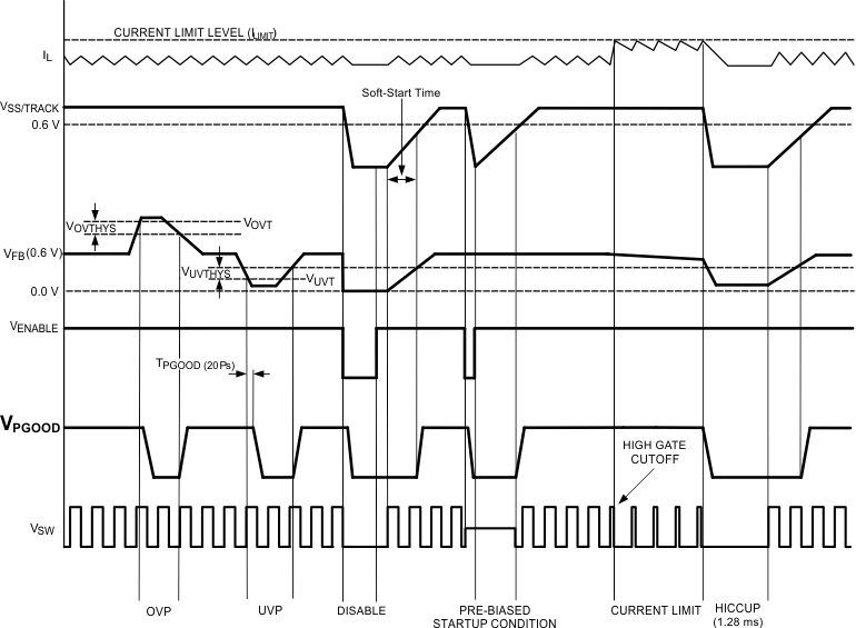
LM27402 30092664.gifFigure 21. Power Good Behavior

The PGOOD flag of the LM27402 is used to signal when the output is out of regulation or during nonregulated pre-biased conditions. This means that current limit, UVLO, overvoltage threshold, undervoltage threshold, or a non-regulated output will cause the PGOOD pin to pull low. To prevent glitches to PGOOD, a 20-μs deglitch filter is built into the LM27402. Figure 21 illustrates when the PGOOD flag is asserted low.