JAJSB09K January 2010 – February 2018 LM27402
PRODUCTION DATA.
- 1 特長
- 2 アプリケーション
- 3 概要
- 4 改訂履歴
- 5 Pin Configuration and Functions
- 6 Specifications
-
7 Detailed Description
- 7.1 Overview
- 7.2 Functional Block Diagram
- 7.3
Feature Description
- 7.3.1 Wide Input Voltage Range
- 7.3.2 UVLO
- 7.3.3 Precision Enable
- 7.3.4 Soft-Start and Voltage Tracking
- 7.3.5 Output Voltage Setpoint and Accuracy
- 7.3.6 Voltage-Mode Control
- 7.3.7 Power Good
- 7.3.8 Inductor-DCR-Based Overcurrent Protection
- 7.3.9 Current Sensing
- 7.3.10 Power MOSFET Gate Drivers
- 7.3.11 Pre-Bias Start-up
- 7.4 Device Functional Modes
-
8 Application and Implementation
- 8.1
Application Information
- 8.1.1 Converter Design
- 8.1.2 Inductor Selection (L)
- 8.1.3 Output Capacitor Selection (COUT)
- 8.1.4 Input Capacitor Selection (CIN)
- 8.1.5 Using Precision Enable
- 8.1.6 Setting the Soft-Start Time
- 8.1.7 Tracking
- 8.1.8 Setting the Switching Frequency
- 8.1.9 Setting the Current Limit Threshold
- 8.1.10 Control Loop Compensation
- 8.1.11 MOSFET Gate Drivers
- 8.1.12 Power Loss and Efficiency Calculations
- 8.2 Typical Applications
- 8.1
Application Information
- 9 Power Supply Recommendations
- 10Layout
- 11デバイスおよびドキュメントのサポート
- 12メカニカル、パッケージ、および注文情報
パッケージ・オプション
メカニカル・データ(パッケージ|ピン)
サーマルパッド・メカニカル・データ
発注情報
8.1.1 Converter Design
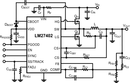
As with any DC/Dc converter, numerous tradeoffs are required to optimize the design for efficiency, size, or performance. Such tradeoffs are highlighted throughout the following discussion. To facilitate component selection, the circuit shown in Figure 26 may be used as a reference. Unless otherwise indicated, all formulae assume units of Amps (A) for current, Farads (F) for capacitance, Henries (H) for inductance and Volts (V) for voltage.
Figure 26 shows RF and CF acting as an RC filter to the VIN pin of the LM27402. The filter is used to attenuate voltage ripple that may exist on the input rail particularly during high output currents. The recommended values of RF and CF are 2.2 Ω and 1 µF, respectively. There is a practical limit to the size of RF as it can cause a large voltage drop if large operating bias currents are present. The VIN pin of the LM27402 must not exceed 150 mV difference from the input voltage rail (VIN).
Equation 1 is used to calculate for any buck converter is duty ratio:

Due to the resistive powertrain losses, the duty ratio will increase based on the overall efficiency, η. Calculation of η can be found in the Power Loss and Efficiency Calculationssection of this data sheet.
 Figure 26. Typical Application Circuit