JAJSRJ1A June 2011 – February 2024 OPA564-Q1
PRODUCTION DATA
- 1
- 1 特長
- 2 アプリケーション
- 3 概要
- 4 Device Comparison Table
- 5 Pin Configuration and Functions
- 6 Specifications
- 7 Detailed Description
- 8 Application and Implementation
- 9 Device and Documentation Support
- 10Revision History
- 11Mechanical, Packaging, and Orderable Information
パッケージ・オプション
メカニカル・データ(パッケージ|ピン)
- DWP|20
サーマルパッド・メカニカル・データ
- DWP|20
発注情報
8.1.4 Power Dissipation and Safe Operating Area
Power dissipation depends on power supply, signal, and load conditions. For dc signals, power dissipation is equal to the product of output current (IOUT) and the voltage across the conducting output transistor [(V+) – VOUT when sourcing; VOUT – (V–) when sinking]. Dissipation with ac signals is lower. See the Power Amplifier Stress and Power Handling Limitations application bulletin, available for download from www.ti.com, for an explanation on how to calculate or measure power dissipation with unusual signals and loads.
Figure 8-2 shows the safe operating area at room temperature with various heat-sinking efforts. Note that the safe output current decreases as (V+) – VOUT or VOUT – (V–) increases. Figure 8-3 shows the safe operating area at various temperatures with the thermal pad being soldered to a 2oz copper pad.


The power that can be safely dissipated in the package is related to the ambient temperature and the heat-sink design. The PowerPAD integrated circuit package was specifically designed to provide excellent power dissipation, but board layout greatly influences the heat dissipation of the package. See Section 8.4.1.1 section for further details.
The relationship between thermal resistance and power dissipation can be expressed as:
Combining these equations produces:
where:
- TJ = Junction temperature (°C)
- TA = Ambient temperature (°C)
- θJA = Junction-to-ambient thermal resistance (°C/W)
- PD = Power dissipation (W)
To determine the required heat-sink area, calculate the required power dissipation and consider the relationship between power dissipation and thermal resistance to minimize shutdown conditions and allow for proper long-term operation (junction temperature of 85°C or less).
After the heat-sink area has been selected, test for worst-case load conditions to maintain proper thermal protection.
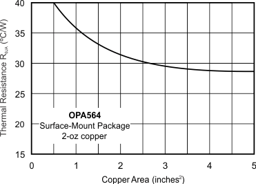
For applications with limited board size, see Figure 8-4 for the approximate thermal resistance relative to heat-sink area. Increasing heat-sink area beyond 2in2 provides little improvement in thermal resistance. To achieve the 28.7°C/W shown in Thermal Information, a 2oz copper plane size of 3in2 is used. The PowerPAD integrated circuit package is designed for continuous power levels from 2W to 4W, depending on ambient temperature and heat-sink area. The addition of airflow also influences maximum power dissipation, as Figure 8-5 illustrates. Higher power levels can be achieved in applications with a low on and off duty cycle, such as remote meter reading.
 Figure 8-4 Thermal Resistance vs
Circuit Board Copper Area
 Figure 8-5 Maximum Power Dissipation
vs Temperature