JAJSSX9I December 2001 – February 2024 OPA656
PRODUCTION DATA
- 1
- 1 特長
- 2 アプリケーション
- 3 概要
- 4 Device Comparison Table
- 5 Pin Configuration and Functions
- 6 Specifications
- 7 Detailed Description
- 8 Application and Implementation
- 9 Device and Documentation Support
- 10Revision History
- 11Mechanical, Packaging, and Orderable Information
パッケージ・オプション
メカニカル・データ(パッケージ|ピン)
サーマルパッド・メカニカル・データ
発注情報
8.2.2 Detailed Design Procedure
Designs that require high bandwidth from a large area detector with relatively high transimpedance gain benefit from the low input voltage noise of the OPA656. This input voltage noise is peaked up over frequency by the diode source capacitance, and can, in many cases, become the limiting factor to input sensitivity. The key elements to the design are the expected diode capacitance (CD) with the reverse bias voltage (VB) applied the desired transimpedance gain, RF, and the GBP for the OPA656 (230 MHz). Figure 8-3 shows a transimpedance circuit with the parameters as described in Table 8-1. With these three variables set (and including the parasitic input capacitance for the OPA656 and the PCB added to CD), the feedback capacitor value (CF) can be set to control the frequency response. To achieve a maximally-flat second-order Butterworth frequency response, set the feedback pole to:
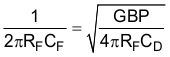
The input capacitance of the amplifier is the sum of the common-mode and differential capacitance (0.4 + 2.6) pF. The parasitic capacitance from the photodiode package and the PCB is approximately 0.3 pF. These values result in a total effective input capacitance of CD = 23.3 pF. From Equation 1, set the feedback pole at 2.8 MHz. Setting the pole at 2.8 MHz requires a total feedback capacitance of 0.57 pF
The approximate −3‑dB bandwidth of the transimpedance amplifier circuit is given by:
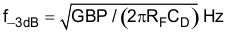
Equation 2 estimates a closed-loop bandwidth of 3.96 MHz. The total feedback capacitance for the circuit used in the design is estimated to be 0.6 pF. The total feedback capacitance includes the physical 0.5 pF feedback capacitor in parallel with 100-fF of parasitic capacitance due to the feedback resistor and PCB trace. The parasitic capacitance from the PCB trace can be minimized by removing the ground and power planes in the feedback path. A TINA SPICE simulation of the circuit in Figure 8-3 results in a closed-loop bandwidth of 4.2 MHz.
Figure 8-4 shows the measured output noise of the system. The low-frequency output noise of 40 nV/√Hz gets input-referred to 0.40 pA/√Hz. The transimpedance gain resistor is the dominant noise source with the operational amplifier contributing a negligible amount, reflecting one of the main benefits in using a JFET input amplifier in a high-gain transimpedance application. If the total output noise of the TIA is band limited to a frequency less than the feedback pole frequency, a very simple expression for the equivalent output noise voltage can be derived by Equation 3.
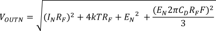
where
- VOUTN = Equivalent output noise when band-limited to F < 1 / (2ΩRfCf)
- IN = Input current noise for the operational amplifier inverting input
- EN = Input voltage noise for the operational amplifier
- CD = Diode capacitance including operational amplifier and PCB parasitic capacitance
- F = Band-limiting frequency in Hz (usually a postfilter before further signal processing)
- 4 kT = 1.6 e – 20 J at T = 290K
Figure 8-5 shows the frequency response of the design. The 4.2‑MHz bandwidth of the circuit approximately matches the theoretical value calculated using Equation 2.