JAJSCW3A December 2016 – February 2020 SN65MLVD206B
PRODUCTION DATA.
- 1 特長
- 2 アプリケーション
- 3 概要
- 4 改訂履歴
- 5 概要(続き)
- 6 Pin Configuration and Functions
-
7 Specifications
- Table 1. Absolute Maximum Ratings
- Table 2. ESD Ratings
- Table 3. Recommended Operating Conditions
- Table 4. Thermal Information
- Table 5. Electrical Characteristics
- Table 6. Electrical Characteristics – Driver
- Table 7. Electrical Characteristics – Receiver
- Table 8. Electrical Characteristics – BUS Input and Output
- Table 9. Switching Characteristics – Driver
- Table 10. Switching Characteristics – Receiver
- 7.1 Typical Characteristics
- 8 Parameter Measurement Information
- 9 Detailed Description
-
10Application and Implementation
- 10.1 Application Information
- 10.2
Typical Application
- 10.2.1 Multipoint Communications
- 10.2.2 Design Requirements
- 10.2.3
Detailed Design Procedure
- 10.2.3.1 Supply Voltage
- 10.2.3.2 Supply Bypass Capacitance
- 10.2.3.3 Driver Input Voltage
- 10.2.3.4 Driver Output Voltage
- 10.2.3.5 Termination Resistors
- 10.2.3.6 Receiver Input Signal
- 10.2.3.7 Receiver Input Threshold (Failsafe)
- 10.2.3.8 Receiver Output Signal
- 10.2.3.9 Interconnecting Media
- 10.2.3.10 PCB Transmission Lines
- 10.2.4 Application Curves
- 11Power Supply Recommendations
- 12Layout
- 13デバイスおよびドキュメントのサポート
- 14メカニカル、パッケージ、および注文情報
10.2.3.7 Receiver Input Threshold (Failsafe)
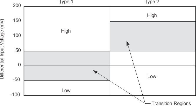
The MLVDS standard defines a Type-1 and Type-2 receiver. Type-1 receivers have their differential input voltage thresholds near zero volts. Type-2 receivers have their differential input voltage thresholds offset from 0 V to detect the absence of a voltage difference. The impact to receiver output by the offset input can be seen in Table 15 and Figure 18.
Table 15. Receiver Input Voltage Threshold Requirements
| RECEIVER TYPE | OUTPUT LOW | OUTPUT HIGH |
|---|---|---|
| Type 1 | –2.4 V ≤ VID ≤ –0.05 V | 0.05 V ≤ VID ≤ 2.4 V |
| Type 2 | –2.4 V ≤ VID ≤ 0.05 V | 0.15 V ≤ VID ≤ 2.4 V |
 Figure 18. Expanded Graph of Receiver Differential Input Voltage Showing Transition Region