SBVS241 April 2014 TLC5954
PRODUCTION DATA.
- 1 Features
- 2 Applications
- 3 Description
- 4 Revision History
- 5 Pin Configuration and Functions
- 6 Specifications
- 7 Parameter Measurement Information
- 8 Detailed Description
- 9 Applications and Implementation
- 10Power Supply Recommendations
- 11Layout
- 12Device and Documentation Support
- 13Mechanical, Packaging, and Orderable Information
パッケージ・オプション
メカニカル・データ(パッケージ|ピン)
- RTQ|56
サーマルパッド・メカニカル・データ
- RTQ|56
発注情報
9 Applications and Implementation
9.1 Application Information
The device is a 48-channel, constant sink current, LED driver. This device is typically connected in series to drive many LED lamps with only a few controller ports. Output current control data and on or off control data can be written from the SIN input pin. The on or off timing can be controlled by the BLANK signal. Also, the LED open and short error flag can be read out from the SOUT output pin.
9.2 Typical Application
In this application, the device VCC and LED lamp anode voltages are supplied from different power supplies.
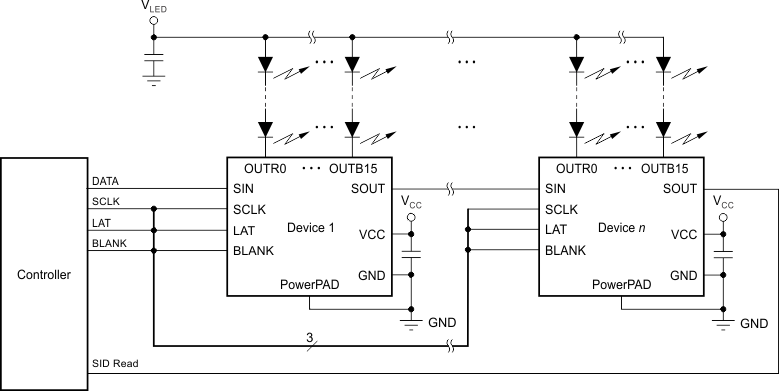 Figure 37. Typical Application Circuit (Multiple Daisy-Chained Devices)
9.2.1 Design Requirements
For this design example, use the following as the input parameters.
Table 11. Design Parameters
| DESIGN PARAMETER | EXAMPLE VALUE |
|---|---|
| VCC input voltage range | 3.0 V to 3.6 V |
| LED lamp (VLED) input voltage range | Maximum LED forward voltage (VF) + 0.4 V (knee voltage) |
| SIN, SCLK, LAT, and BLANK voltage range | Low level = GND, high level = VCC |
9.2.2 Detailed Design Procedure
9.2.2.1 Step-by-Step Design Procedure
To begin the design process, a few parameters must be decided upon. The designer needs to know the following:
- Maximum output constant-current value for all colors of the LED ramp.
- Maximum LED forward voltage (VF).
- Current ratio of red, green, and blue LED lamps for the best white balance.
- Is the LED open detect (LOD) function used? If so, which detection level (0.20 V, 0.30 V, 0.40 V, 0.50 V, or 0.60 V) is used?
- Is the LED short detect (LSD) function used? If so, which detection level (50% VCC, 70% VCC, or 90% VCC) is used?
9.2.2.2 Maximum Current (MC) Data
There are a total of three bits of MC data that set the output current of all constant-current outputs (OUTXn). Select the MC data to be greater than the target LED ramp current if the output current is reduced white balanced by the global brightness control data and write the data with other control data.
9.2.2.3 Global Brightness Control (BC) Data
There are a total of three sets of 7-bit BC data for the red, green, and blue LED ramp. Select the BC data for the best white balance of the red, green, and blue LED ramp and write the data with other control data.
9.2.2.4 On or Off Data
There are a total of 48 bits of on or off data for the on or off control of each output. Select the on or off data of the LED lamp on or off status control and write the data.
9.2.2.5 Other Control Data
There are a total of 8 bits of control data to set the function mode for the status information data (SID) load control, LOD voltage setting, LSD voltage setting, and power save mode (PSM) explained in the Device Functional Modes section. Write the 8-bit control data for the appropriate operation of the display system with MC and BC data as the control data.
9.2.2.6 Grayscale Control
All constant-current outputs are controlled by the BLANK pin logic level. When BLANK is GND, all constant-current outputs are turned on except that the output is set to 0 in the 48-bit output on-off data latch. When BLANK is VCC, all outputs are forced off. The LED lamp grayscale can be controlled by the BLANK low pulse duration.
9.2.3 Application Curves
One LED connected to each output. BLANK low pulse duration = 40 ns.
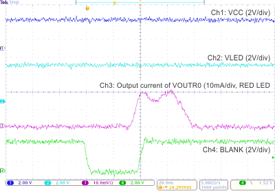
| MCX = 5 | BCX = 7Fh | VLED = 4.2 V |
| VCC = 3.3 V | SIDLD = LODVLT = LSDVLT = PSMODE = 0 | |
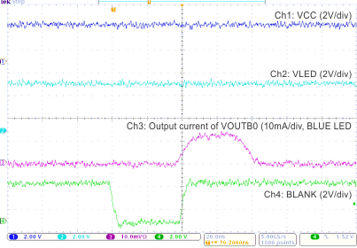
| MCX = 5 | BCX = 7Fh | VLED = 4.2 V | ||
| VCC = 3.3 V | SIDLD = LODVLT = LSDVLT = PSMODE = 0 | |||
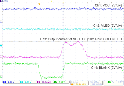
| MCX = 5 | BCX = 7Fh | VLED = 4.2 V |
| VCC = 3.3 V | SIDLD = LODVLT = LSDVLT = PSMODE = 0 | |