SBVS241 April 2014 TLC5954
PRODUCTION DATA.
- 1 Features
- 2 Applications
- 3 Description
- 4 Revision History
- 5 Pin Configuration and Functions
- 6 Specifications
- 7 Parameter Measurement Information
- 8 Detailed Description
- 9 Applications and Implementation
- 10Power Supply Recommendations
- 11Layout
- 12Device and Documentation Support
- 13Mechanical, Packaging, and Orderable Information
パッケージ・オプション
メカニカル・データ(パッケージ|ピン)
- RTQ|56
サーマルパッド・メカニカル・データ
- RTQ|56
発注情報
7 Parameter Measurement Information
7.1 Pin Equivalent Input and Output Schematic Diagrams
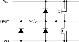 Figure 16. SIN, SCLK, LAT, BLANK
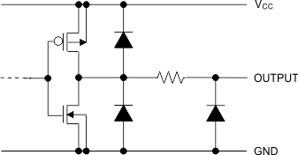 Figure 17. SOUT
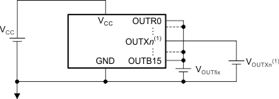
1. X = R, G, or B. n = 0 to 15.
Figure 18. OUTXn7.2 Test Circuits
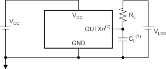
1. CL includes measurement probe and jig capacitance.
2. X = R, G, or B. n = 0 to 15.
Figure 19. Rise and Fall Time Test Circuit for OUTXn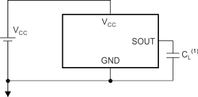
1. CL includes measurement probe and jig capacitance.
Figure 20. Rise and Fall Time Test Circuit for SOUT
1. X = R, G, or B. n = 0 to 15.
Figure 21. Constant-Current Test Circuit for OUTXn7.3 Timing Diagrams
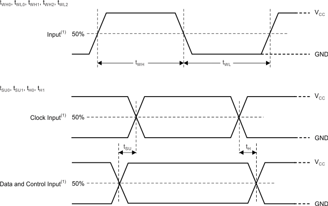
1. Input pulse rise and fall time is 1 ns to 3 ns.
Figure 22. Input Timing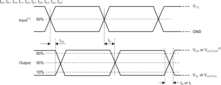
1. Input pulse rise and fall time is 1 ns to 3 ns.
2. X = R, G, or B. n = 0 to 15.
Figure 23. Output Timing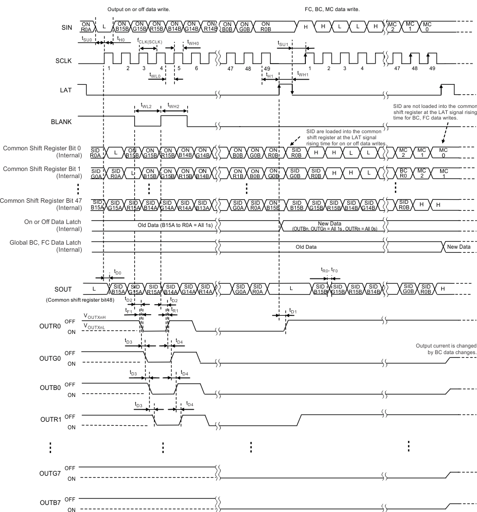
1. X = R, G, or B. n = 0 to 15.
Figure 24. Data Write and OUTXn On or Off Timing Diagram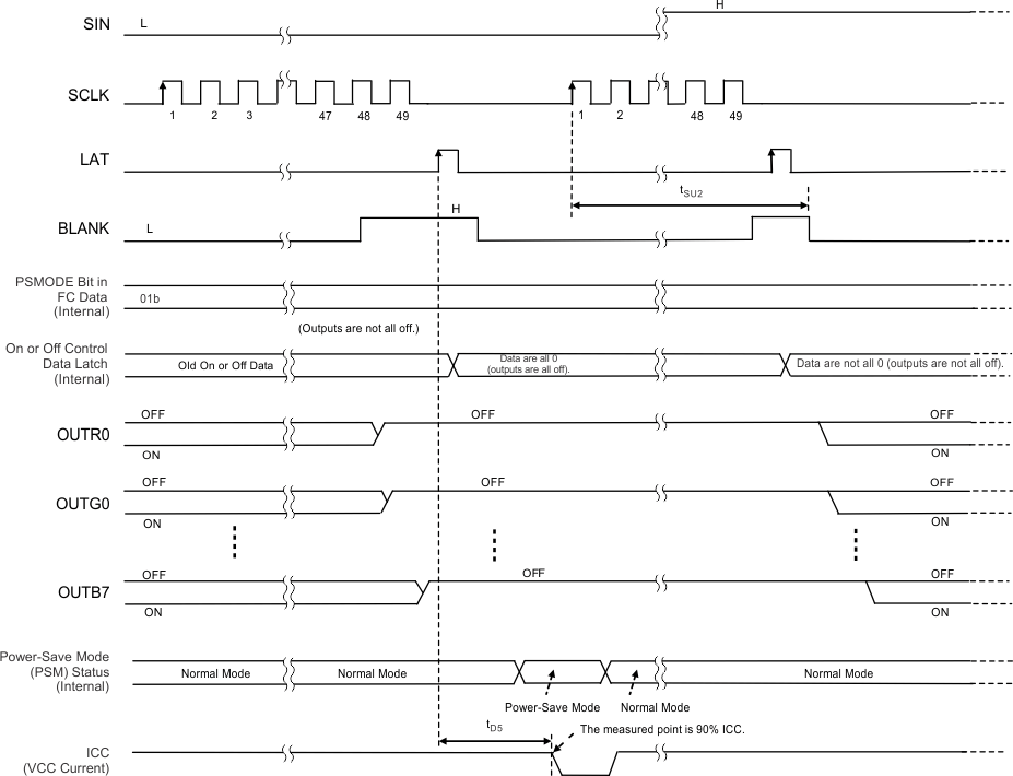 Figure 25. Power-Save Mode Timing Diagram (PSMODE = 01b)
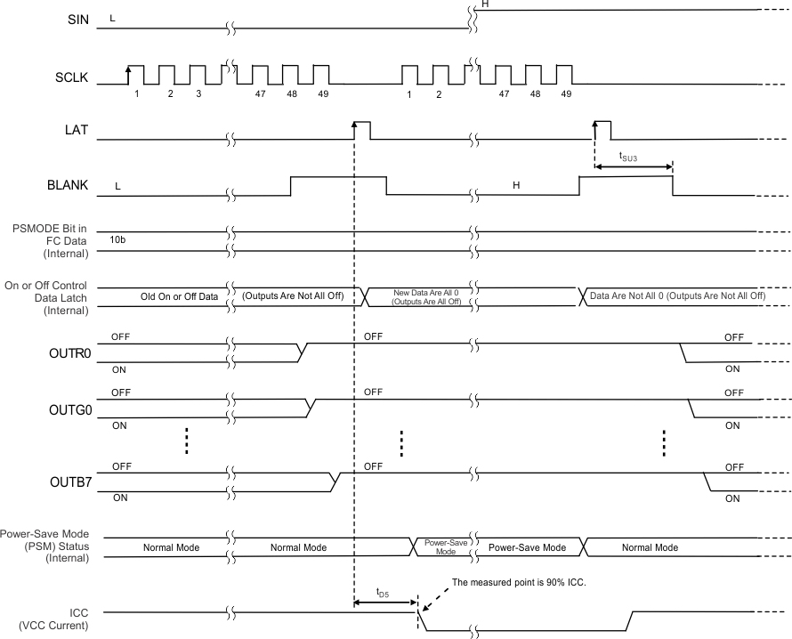 Figure 26. Power-Save Mode Timing Diagram (PSMODE = 10b)