SBVS241 April   2014 TLC5954

PRODUCTION DATA.  

  1. Features
  2. Applications
  3. Description
  4. Revision History
  5. Pin Configuration and Functions
  6. Specifications
    1. 6.1 Absolute Maximum Ratings
    2. 6.2 Handling Ratings
    3. 6.3 Recommended Operating Conditions
    4. 6.4 Thermal Information
    5. 6.5 Electrical Characteristics
    6. 6.6 Switching Characteristics
    7. 6.7 Typical Characteristics
  7. Parameter Measurement Information
    1. 7.1 Pin Equivalent Input and Output Schematic Diagrams
    2. 7.2 Test Circuits
    3. 7.3 Timing Diagrams
  8. Detailed Description
    1. 8.1 Overview
    2. 8.2 Functional Block Diagram
    3. 8.3 Feature Description
      1. 8.3.1 Output Current Calculation
      2. 8.3.2 Status Information Data (SID)
      3. 8.3.3 LED Open Detection (LOD)
      4. 8.3.4 LED Short Detection (LSD)
      5. 8.3.5 Noise Reduction
    4. 8.4 Device Functional Modes
      1. 8.4.1 Maximum Constant Sink Current
      2. 8.4.2 Global Brightness Control (BC) Function: Sink Current Control
      3. 8.4.3 Constant-Current Output On or Off Control
      4. 8.4.4 Power-Save Mode
    5. 8.5 Register Maps
      1. 8.5.1 Register and Data Latch Configuration
        1. 8.5.1.1 Common Shift Register
        2. 8.5.1.2 Output On or Off Data Latch
        3. 8.5.1.3 Maximum Current Control (MC), Global Brightness Control (BC), and Function Control (FC) Data Latch
  9. Applications and Implementation
    1. 9.1 Application Information
    2. 9.2 Typical Application
      1. 9.2.1 Design Requirements
      2. 9.2.2 Detailed Design Procedure
        1. 9.2.2.1 Step-by-Step Design Procedure
        2. 9.2.2.2 Maximum Current (MC) Data
        3. 9.2.2.3 Global Brightness Control (BC) Data
        4. 9.2.2.4 On or Off Data
        5. 9.2.2.5 Other Control Data
        6. 9.2.2.6 Grayscale Control
      3. 9.2.3 Application Curves
  10. 10Power Supply Recommendations
  11. 11Layout
    1. 11.1 Layout Guidelines
    2. 11.2 Layout Example
  12. 12Device and Documentation Support
    1. 12.1 Device Support
      1. 12.1.1 Development Support
    2. 12.2 Documentation Support
      1. 12.2.1 Related Documentation
    3. 12.3 Trademarks
    4. 12.4 Electrostatic Discharge Caution
    5. 12.5 Glossary
  13. 13Mechanical, Packaging, and Orderable Information

パッケージ・オプション

メカニカル・データ(パッケージ|ピン)
サーマルパッド・メカニカル・データ
発注情報

11 Layout

11.1 Layout Guidelines

  1. The decoupling capacitor should be placed near the VCC and GND pin.
  2. The GND pattern should be routed as widely as possible for large GND currents. Maximum GND current is approximately 1.52 A.
  3. The routing between the LED cathode side and the device OUTXn should be routed to be as short and straight as possible to reduce wire inductance.
  4. The PowerPAD should be connected to the GND layer because the pad is connected to GND internally. The PowerPAD also should be connected to the heat sink layer to reduce device temperature.

11.2 Layout Example

ai_layout_sbvs241.gif
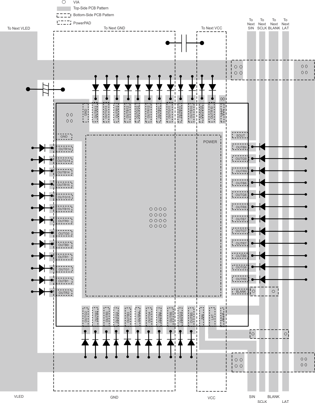
Figure 41. Layout Example