SBVS241 April 2014 TLC5954
PRODUCTION DATA.
- 1 Features
- 2 Applications
- 3 Description
- 4 Revision History
- 5 Pin Configuration and Functions
- 6 Specifications
- 7 Parameter Measurement Information
- 8 Detailed Description
- 9 Applications and Implementation
- 10Power Supply Recommendations
- 11Layout
- 12Device and Documentation Support
- 13Mechanical, Packaging, and Orderable Information
パッケージ・オプション
メカニカル・データ(パッケージ|ピン)
- RTQ|56
サーマルパッド・メカニカル・データ
- RTQ|56
発注情報
8 Detailed Description
8.1 Overview
The TLC5954 is 48-channel, 34.9-mA or 24.4-mA, constant-current LED driver that can control the LED on of off settings with the BLANK signal for grayscale (GS) control. The minimum 40-ns BLANK signal pulse duration can be input to generate very short LED on-time.
The device has a 128-step, 7-bit, output current control function termed global brightness control (BC) that can control each color group output. The BC function can adjust the red, green, and blue LED intensity for true white with constant-current control. The device contributes higher image quality to LED displays with fine white balance tuning by using these BLANK pulse durations and MC, BC functions.
The display controller can locate LED lamp failures via the device because the controller can detect LED lamp failures with the LED open detection (LOD) and LED short detection (LSD) functions. Furthermore, the reliability of the display can be improved by the LOD and LSD function.
The device maximum constant-current output value can be set by an internal register data function referred to as maximum current control (MC), instead of the general method of using an external resistor setting. Thus, any failure modes that occur from the external resistor can be eliminated. One resistor can also be eliminated with the MC function.
The device constant-current output can drive approximately 17.4 mA at a 0.32-V output voltage and a +25°C ambient temperature. This voltage is called knee voltage. This 0.32-V, low-knee voltage can contribute to the design of a lower-power display system.
The total number of LED drivers on one LED display panel can be reduced because 48 LED lamps can be driven by one LED driver. Therefore, designing fine-pitch LED displays is simplified.
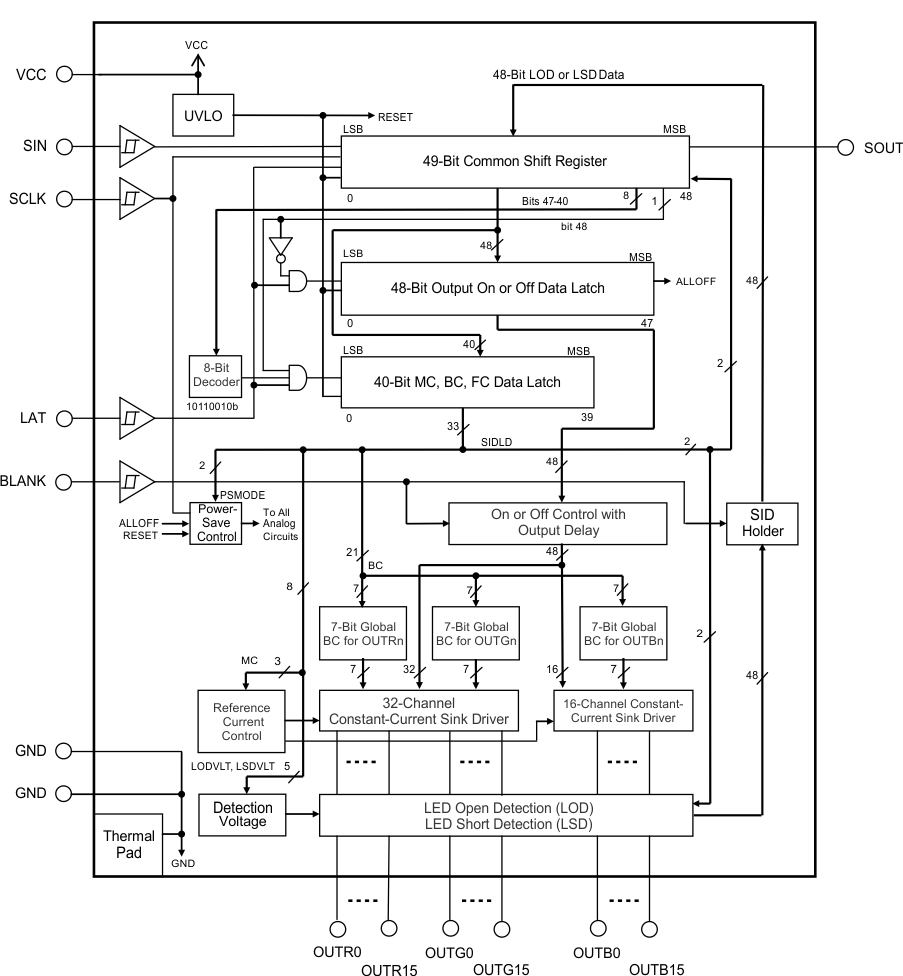
8.2 Functional Block Diagram
8.3 Feature Description
8.3.1 Output Current Calculation
The output current value controlled by MC and BC can be calculated by Equation 1.
where
- IOLCMax = the maximum constant-current value for all OUTXn for each color group programmed by MC data,
- BCX = the global brightness control value (0h to 7Fh),
- X = R, G, or B for the red, green, or blue color group, and
- n = 0 to 15.
Each output sinks the IOLCMax current when they turn on and the global brightness control (BC) data are set to the maximum value of 7Fh (127d).
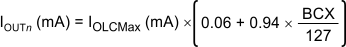
8.3.2 Status Information Data (SID)
The status information data (SID) contains the status of the LED open detection (LOD) and LED short detection (LSD).
When the output on-off data latch is written, the SID selected by the SIDLD bits are loaded into lower 48 bits in the common shift register at the LAT rising edge after the original data in the common shift register are copied to the on-off data latch. When the BC and FC data are written, SID data are not loaded to the common shift register. After SID data are copied into the common shift register, new SID data are not loaded until new data are written into the common shift register even if a LAT rising edge is input.
When the device resumes normal operation after the power-save mode, a BLANK rising edge must be input after tSU2 or tSU3 elapses in order to retain correct LOD and LSD data in the SID holder because the SID analog circuit does not function during power-save mode. The SID load configuration and SID read timing are shown in Figure 27 and Figure 28, respectively.
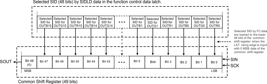 Figure 27. SID Load Configuration
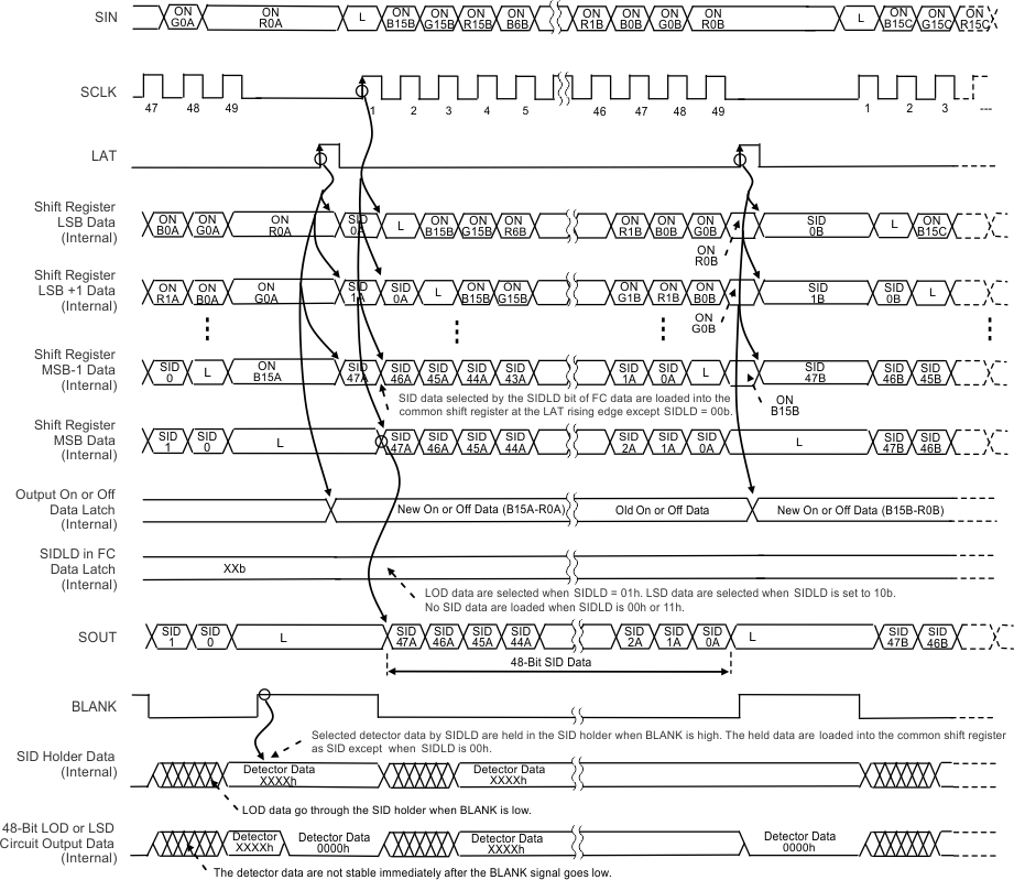 Figure 28. SID Read Timing Diagram
8.3.3 LED Open Detection (LOD)
LOD detects a fault caused by an open circuit in the nth LED string, or a short from OUTXn to ground with low impedance, by comparing the OUTXn voltage to the LOD detection threshold voltage level set by LODVLT in the function control data latch (see Table 6 and Table 8). If the OUTXn voltage is lower than the programmed voltage, the corresponding output LOD bit is set to 1 to indicate a shorted LED. Otherwise, the LOD bit is set to 0. LOD data are only valid for outputs that are set to 1 in the output on-off data latch. LOD data are always 0 for outputs that are set to 0 in the output on-off data latch.
LOD data are stored in a 48-bit register called the SID holder (see the Functional Block Diagram) at the BLANK rising edge when the SIDLD bits are set to 01b (see Table 7). The loaded LOD data can be read out through the common shift register as SID data at the SOUT pin. LOD data are not valid for 1 μs after the output is turned on. If the OUTXn controlled by the BLANK pin is less than 1 µs, the LOD data must be ignored.
When the device resumes operation from power-save mode, all OUTXn can be controlled by the internal on-off control data and the BLANK level after the setup time (tSU2) elapses. LOD data are valid after the propagation delay. Figure 29 illustrates an LOD and LSD circuit, Table 1 shows the SID bit settings for LOD and LSD, and Figure 30 illustrates the LED open-detection operating timing diagram.
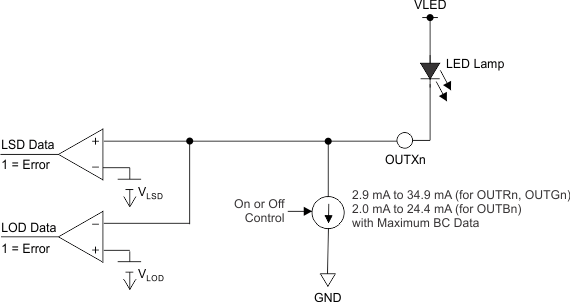 Figure 29. LOD, LSD Circuit
Table 1. LOD, LSD Truth Table
| LOD | LSD | CORRESPONDING BIT IN SID |
|---|---|---|
| LED is not open (VOUTXn > VLOD) | LED is not shorted (VOUTXn ≤ VLSD) | 0 |
| LED is open or shorted to GND (VOUTXn ≤ VLOD) | LED is shorted between anode and cathode, or shorted to higher voltage side (VOUTXn > VLSD) | 1 |
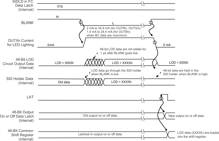 Figure 30. LOD Operation Timing Diagram
8.3.4 LED Short Detection (LSD)
LSD data detect a fault caused by a shorted LED by comparing the OUTXn voltage to the LSD detection threshold voltage level set by LSDVLT in the function control data latch (see Table 6 and Table 9). If the OUTXn voltage is higher than the programmed voltage, the corresponding output LSD bit is set to 1 to indicate a shorted LED. Otherwise, the LSD bit is set to 0. LSD data are only valid for outputs that are set to 1 in the output on-off data latch. LSD data are always 0 for outputs that are set to 0 in the output on-off data latch.
LSD data are loaded into a 48-bit register called the SID holder at the BLANK rising edge when the SIDLD bits are set to 10b (see Table 7). The loaded LSD data can be read out through the common shift register as SID data at the SOUT pin. LSD data are not valid for 1 μs after the output is turned on. If the OUTXn controlled by the BLANK pin is less than 1 µs, the LSD data must be ignored.
When the device resumes operation from power-save mode, all OUTXn can be controlled by the internal on-off control data and the BLANK level after the setup time (tSU2) elapses. LSD data are valid after the propagation delay. Figure 29 illustrates an LOD and LSD circuit and Figure 31 shows LED short-detection operating timing diagram.
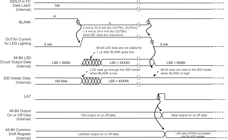 Figure 31. LSD Operation Timing Diagram
8.3.5 Noise Reduction
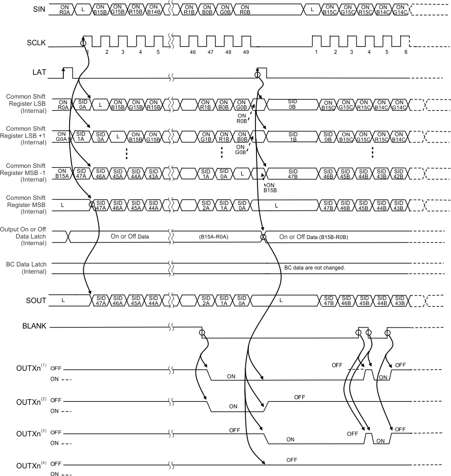
Large surge currents may flow through the device and the board on which the device is mounted if all 48 LED channels turned on simultaneously when BLANK toggles from high to low. These large current surges can induce detrimental noise and electromagnetic interference (EMI) into other circuits. The device turns on the LED channels in a series delay to provide a circuit soft-start feature. A small delay circuit is implemented between each output. When all bits of the on-off data latch are set to 1, each constant-current output turns on in the following order: OUTR0, OUTG0, OUTB0, OUTR15, OUTG15, OUTB15, OUTR1, OUTG1, OUTB1, OUTR14, OUTG14, OUTB14, OUTR2, OUTG2, OUTB2, OUTR13, OUTG13, OUTB13, OUTR3, OUTG3, OUTB3, OUTR12, OUTG12, OUTB12, OUTR4, OUTG4, OUTB4, OUTR11, OUTG11, OUTB11, OUTR5, OUTG5, OUTB5, OUTR10, OUTG10, OUTB10, OUTR6, OUTG6, OUTB6, OUTR9, OUTG9, OUTB9, OUTR7, OUTG7, OUTB7, OUTR8, OUTG8, and OUTB8 with a small delay for each OUTXn after BLANK goes low or LAT goes high, see Figure 24. Both turn-on and turn-off times are delayed.
8.4 Device Functional Modes
8.4.1 Maximum Constant Sink Current
The maximum output current of each channel (IOLCMax) is programmed by maximum current (MC) data and can be set by the serial interface.
IOLCMax is the highest current for each output. Each OUTXn sinks IOLCMax current when they turn on with the global brightness control (BC) data set to the maximum value of 7Fh (127d). MC data are updated when the same data are written to the MC bits twice. When the device is powered on, the MC data latch is set to 0.
Table 2 shows the characteristics of the constant-current sink versus the MC control data.
Table 2. Maximum Constant-Current Output versus MC Data
| MC DATA | IOLCMax (mA) | |||
|---|---|---|---|---|
| BINARY | DECIMAL | HEX | OUTRn, OUTGn | OUTBn |
| 000 (default) | 0 (default) | 0 (default) | 2.9 | 2.0 |
| 001 | 1 | 1 | 4.4 | 3.1 |
| 010 | 2 | 2 | 5.8 | 4.1 |
| 011 | 3 | 3 | 8.7 | 6.1 |
| 100 | 4 | 4 | 11.6 | 8.1 |
| 101 | 5 | 5 | 17.4 | 12.2 |
| 110 | 6 | 6 | 23.2 | 16.3 |
| 111 | 7 | 7 | 34.9 | 24.4 |
8.4.2 Global Brightness Control (BC) Function: Sink Current Control
The device is capable of simultaneously adjusting the output current of each color group (OUTR0 to OUTR15, OUTG0 to OUTG15, and OUTB0 to OUTB15). This function is called global brightness control (BC). The BC function allows the global BC data of LEDs connected to the three color groups to be adjusted. All OUTXn can be adjusted in 128 steps from 6% to 100% of the maximum output current, IOLCMax. The BC data are transmitted to the device by the serial interface. When BC data change, the output current also changes immediately.
Table 3 shows the BC data versus the constant-current ratio against IOLCMax.
Table 3. BC Data versus Current Ratio and Set Current Value
| BC DATA | OUTPUT CURRENT RATIO TO IOLCMax (%, typ) |
OUTPUT CURRENT (mA, typ) | ||||||
|---|---|---|---|---|---|---|---|---|
| BINARY | DECIMAL | HEX | OUTRn, OUTGn | OUTBn | ||||
| MSB | LSB | MC = 7h (IOLCMax = 34.9 mA) |
MC = 0h (IOLCMax = 2.9 mA) |
MC = 7h (IOLCMax = 24.4 mA) |
MC = 0h (IOLCMax = 2.0 mA) |
|||
| 000 | 0000 | 0 | 00 | 6.0 | 2.09 | 0.17 | 1.47 | 0.12 |
| 000 | 0001 | 1 | 01 | 6.7 | 2.35 | 0.20 | 1.65 | 0.14 |
| 000 | 0010 | 2 | 02 | 7.5 | 2.61 | 0.22 | 1.83 | 0.15 |
| … | … | … | … | … | … | … | … | |
| 111 | 1101 | 125 | 7D | 98.5 | 34.4 | 2.86 | 24.1 | 1.96 |
| 111 | 1110 | 126 | 7E | 99.3 | 34.7 | 2.88 | 24.3 | 1.98 |
| 111 | 1111 | 127 | 7F | 100.0 | 34.9 | 2.90 | 24.4 | 2.00 |
8.4.3 Constant-Current Output On or Off Control
When BLANK is low, each OUTXn is controlled by the data in the output on or off data latch. When data corresponding to an output equal 1, the output turns on; when data corresponding to an output equal 0, the output turns off. When BLANK is high, all OUTXn are forced off. When the device is powered on, the data in the output on or off data latch are set to 0. A truth table for the on or off control data is shown in Table 4.
Table 4. On or Off Control Data Truth Table
| ON OR OFF CONTROL DATA | CONSTANT-CURRENT OUTPUT STATUS |
|---|---|
| 0 (default) | Off |
| 1 | On |
8.4.4 Power-Save Mode
The power-save mode control bits are assigned in the BC and FC data latch. The device dissipation current becomes 7 μA (typ) in this mode. In PSM, all analog circuits (such as the constant-current outputs and the LOD and LSD circuit) do not function. However, logic circuits (such as the common shift register, on-off data latch, and BC and FC data latch) do function. When the two bits in PSMODE are 01b, 10b, or 11b, the power-save mode is enabled. When the two bits are 11b, the device is always in power-save mode. When the two bits are set to 00b, the device is always in normal operation. If all 0s are written in the output on-off data latch, the device goes into power-save mode when the two bits are 01b or 10b. When a rising edge is generated at SCLK with the two PSMODE bits set to 01b, the device exits PSM and returns to normal operation. When data in the output on-off data latch are not all 0s, and when the two PSMODE bits set to 10b, the device exits PSM and returns to normal operation. All OUTXn are turned on after the device exits PSM. Figure 32 and Figure 33 provide power-save mode timing diagrams for PSMODE set to 01b and 10b, respectively. The BLANK level should go low after tSU2 or tSU3 when the device exists PSM and returns to normal mode because the output current may be unstable immediately after starting normal mode.
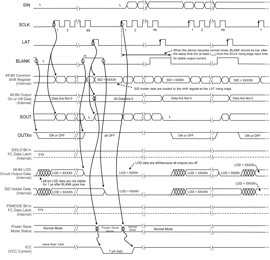 Figure 32. Power-Save Mode (FC Data PSMODE Bits = 01b)
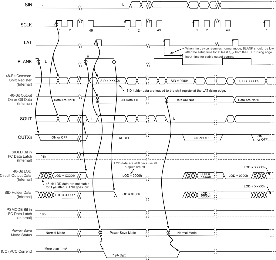 Figure 33. Power-Save Mode (FC Data PSMODE Bits = 10b)
8.5 Register Maps
8.5.1 Register and Data Latch Configuration
The device has one common shift register and four control data latches. These data latches are the output on or off data latch, the maximum current control (MC) data latch, the global brightness control (BC) data latch, and the function control (FC) data latch.
The common shift register is 49 bits long, the output on or off data latch is 48 bits long, and another 48-bit data latch is comprised of the 40-bit MC, BC, and FC data latches with an 8-bit write command decoder. If the common shift register MSB is 0, the least significant 48 bits of data from the 49-bit common shift register are latched into the output on or off data latch. If the MSB (bit 48) from the 49-bit common shift register is 1 and MSB 1 through MSB 9 (bits [47:40]) are 96h (10010110b) for the write command data, the middle 37 bits (bits [39:3]) in the common shift register are latched into the BC and FC data latch. MC data are updated when the same data are written to the MC bits twice with the write command data (96h) and the MSB (bit 48) set to 1. Figure 34 shows the configuration of the common shift register and the four data latches.
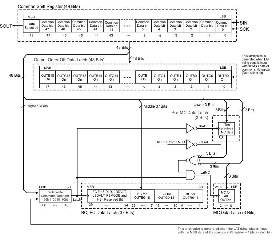 Figure 34. Common Shift Register and Data Latch Configuration
8.5.1.1 Common Shift Register
The 49-bit common shift register is used to shift data from the SIN pin into the device. The data shifted into the register are used for the output on or off control, MC, BC, and several FC functions, and the write command. The LSB of the common shift register is connected to SIN and the MSB is connected to SOUT. On each SCLK rising edge, the data on SIN are shifted into the LSB and all 49 bits are shifted towards the MSB. The register MSB is always connected to SOUT. In addition, the status information data (SID) selected by the SIDLD bits in the FC data latch are loaded to the lower 48 bits of the 49-bit common shift register when a rising edge is input on LAT for the output on or off control data write operation except when SIDLD = 00b and 11b (see Table 7). When the device is powered on, all 49 bits of the common shift register are set to 0.
8.5.1.2 Output On or Off Data Latch
The output on or off data latch is 48 bits long and sets the on or off status for each constant-current output (OUTRn, OUTGn, OUTBn). When BLANK is low, the output corresponding to the specific bit in the output on or off data latch is turned on if the data are 1 and remains off if the data are 0. When BLANK is high, all outputs are forced off, but the data in the latch do not change as long as LAT does not latch in new data. When the MSB of the common shift register is set to 0, the lower 48 bits are written to the output on or off data latch on the LAT rising edge. When the device is powered on, all bits in the data latch are set to 0. The output on or off data latch bit assignment is shown in Table 5. See Figure 35 for an output on or off data write timing diagram.
Table 5. On or Off Control Data Latch Bit Assignment
| BIT NUMBER | BIT NAME | CONTROLLED CHANNEL | DESCRIPTION | BIT NUMBER | BIT NAME | CONTROLLED CHANNEL | DESCRIPTION |
|---|---|---|---|---|---|---|---|
| 0 | OUTR0ON | OUTR0 | 0 = Output off 1 = Output on with BLANK low. When the device is powered on, all bits are set to 0. |
24 | OUTR8ON | OUTR8 | 0 = Output off 1 = Output on with BLANK low. When the device is powered on, all bits are set to 0. |
| 1 | OUTG0ON | OUTG0 | 25 | OUTG8ON | OUTG8 | ||
| 2 | OUTB0ON | OUTB0 | 26 | OUTB8ON | OUTB8 | ||
| 3 | OUTR1ON | OUTR1 | 27 | OUTR9ON | OUTR9 | ||
| 4 | OUTG1ON | OUTG1 | 28 | OUTG9ON | OUTG9 | ||
| 5 | OUTB1ON | OUTB1 | 29 | OUTB9ON | OUTB9 | ||
| 6 | OUTR2ON | OUTR2 | 30 | OUTR10ON | OUTR10 | ||
| 7 | OUTG2ON | OUTG2 | 31 | OUTG10ON | OUTG10 | ||
| 8 | OUTB2ON | OUTB2 | 32 | OUTB10ON | OUTB10 | ||
| 9 | OUTR3ON | OUTR3 | 33 | OUTR11ON | OUTR11 | ||
| 10 | OUTG3ON | OUTG3 | 34 | OUTG11ON | OUTG11 | ||
| 11 | OUTB3ON | OUTB3 | 35 | OUTB11ON | OUTB11 | ||
| 12 | OUTR4ON | OUTR4 | 36 | OUTR12ON | OUTR12 | ||
| 13 | OUTG4ON | OUTG4 | 37 | OUTG12ON | OUTG12 | ||
| 14 | OUTB4ON | OUTB4 | 38 | OUTB12ON | OUTB12 | ||
| 15 | OUTR5ON | OUTR5 | 39 | OUTR13ON | OUTR13 | ||
| 16 | OUTG5ON | OUTG5 | 40 | OUTG13ON | OUTG13 | ||
| 17 | OUTB5ON | OUTB5 | 41 | OUTB13ON | OUTB13 | ||
| 18 | OUTR6ON | OUTR6 | 42 | OUTR14ON | OUTR14 | ||
| 19 | OUTG6ON | OUTG6 | 43 | OUTG14ON | OUTG14 | ||
| 20 | OUTB6ON | OUTB6 | 44 | OUTB14ON | OUTB14 | ||
| 21 | OUTR7ON | OUTR7 | 45 | OUTR15ON | OUTR15 | ||
| 22 | OUTG7ON | OUTG7 | 46 | OUTG15ON | OUTG15 | ||
| 23 | OUTB7ON | OUTB7 | 47 | OUTB15ON | OUTB15 |
Table 6. MC, BC, and FC Data Latch and Write Command Bit Description
| BIT NUMBER |
BIT NAME |
DEFAULT VALUE (BINARY) |
DESCRIPTION |
|---|---|---|---|
| [2:0] | MAXCUR (MC) | 000b | Maximum current control (MC) data for all OUTXn (data = 0h to 7h, see Table 2) |
| [9:3] | BCR (BC) | — | Global brightness control (BC) data for RED color group (data = 00h to 7Fh, see Table 3) |
| [16:10] | BCG (BC) | — | Global brightness control (BC) data for GREEN color group (data = 00h to 7Fh, see Table 3) |
| [23:17] | BCB (BC) | — | Global brightness control (BC) data for BLUE color group (data = 00h to 7Fh, see Table 3) |
| [25:24] | SIDLD (FC) | — | SID load control. These two bits select the SID loaded to the common register when the LAT rising edge is input for on or off data writes. Table 7 shows the selected data truth table. |
| [28:26] | LODVLT (FC) | — | LOD detection voltage select. These three bits select the detection threshold voltage for the LED open detection (LOD). Table 8 shows the detect voltage truth table. |
| [30:29] | LSDVLT (FC) | — | LSD detection voltage select. These two bits select the detection threshold voltage for the LED short detection (LSD). Table 9 shows the detect voltage truth table. |
| [32:31] | PSMODE (FC) | 11b | Power-save mode select. These two bits select the power-save mode between the four modes. Table 10 shows the power-save mode truth table. Figure 32 and Figure 33 illustrate the power-save mode operation timing diagrams. |
| [39:33] | RSV | — | Reserved data, don’t care. |
| [47:40] | WRTCMD | — | Write command. When this data are 96h (10010110b), MC, BC, and FC data can be updated. In order to update MC data, the same data must be written twice to the MC bit. |
Table 7. SID Load Control Truth Table
| SIDLD | STATUS INFORMATION DATA (SID) LOADED TO THE COMMON SHIFT REGISTER | |
|---|---|---|
| BIT 25 | BIT 24 | |
| 0 | 0 | No data are loaded (default value) |
| 0 | 1 | LED open detection (LOD) data are loaded |
| 1 | 0 | LED short detection (LSD) data are loaded |
| 1 | 1 | No data are loaded |
Table 8. LOD Threshold Voltage Truth Table
| LODVLT | LED OPEN DETECTION (LOD) THRESHOLD VOLTAGE | ||
|---|---|---|---|
| BIT 28 | BIT 27 | BIT 26 | |
| 0 | 0 | 0 | VLOD0 (0.20 V, typ) |
| 0 | 0 | 1 | VLOD1 (0.30 V, typ) |
| 0 | 1 | 0 | VLOD2 (0.40 V, typ) |
| 0 | 1 | 1 | VLOD3 (0.50 V, typ) |
| 1 | 0 | 0 | VLOD4 (0.60 V, typ) |
| 1 | 0 | 1 | VLOD1 (0.30 V, typ) |
| 1 | 1 | 0 | VLOD1 (0.30 V, typ) |
| 1 | 1 | 1 | VLOD1 (0.30 V ,typ) |
Table 9. LSD Threshold Voltage Truth Table
| LSDVLT | LED SHORT DETECTION (LSD) THRESHOLD VOLTAGE | |
|---|---|---|
| BIT 30 | BIT 29 | |
| 0 | 0 | VLSD0 (0.50 × VCC, typ) |
| 0 | 1 | VLSD1 (0.70 × VCC, typ) |
| 1 | 0 | VLSD2 (0.90 × VCC, typ) |
| 1 | 1 | VLSD2 (0.90 × VCC, typ) |
Table 10. Power-Save Mode Truth Table
| PSMODE | POWER-SAVE MODE FUNCTION | |
|---|---|---|
| BIT 32 | BIT 31 | |
| 0 | 0 | Power-save mode is disabled in every condition. |
| 0 | 1 | When all zeroes (0s) are written to the output on or off data latch, the device goes to power-save mode. When an SCLK rising edge occurs, the device goes to normal operation and starts to control the output current. However, after the setup time (tSU2) elapses from the SCLK input timing, BLANK must go low. Otherwise, the output current may not reach the set constant-current value. If these two bits are set to 01b from 10b or 11b when the device is in power-save mode (PSM), the device remains in PSM and does not resume normal mode. When an SCLK rising edge is input after PSMODE = 01 is selected, the device returns to normal mode. |
| 1 | 0 | When all zeroes (0s) are written to the output on or off data latch, the device goes to power-save mode. When the data (except all 0s) are written to the output on or off data latch, the device goes to normal operation and starts to control the output current. However, after the setup time (tSU3) elapses from the LAT input timing, BLANK must go low. Otherwise, the output current may not reach the set constant-current value. If this bit set is selected from other bit set to this bit set when the device is in PSM, the device remains in power-save mode. When data that are not all set to off are written to the on or off data latch after this bit set is selected, the device goes to normal mode. |
| 1 (default) | 1 (default) | Power-save mode is enabled in every condition. |
8.5.1.3 Maximum Current Control (MC), Global Brightness Control (BC), and Function Control (FC) Data Latch
The MC, BC, and FC data latch (FC contains the PSMODE, LSDVLT, LODVLT, and SIDLD bits) is 40 bits long and is used to adjust the output current of all OUTXn (OUTRn, OUTGn, OUTBn), to select the status information data (SID) load data, to select LED open detection (LOD) and LED short detection (LSD) voltage, and to select the power-save mode (PSM).
Data are latched from the lower 40 bits of the 49-bit common shift register into the MC, BC, and FC data latch at the LAT rising edge when the MSB of the common shift register is set to 1 and the MSB 1 to MSB 9 bit data (bits [47:40]) of the common shift register MSB side is 96h (10010110b). However, MC data are only updated when the same data as the previous written data are written. Table 6 lists the MC, BC, and FC data latch bit assignment. The MC, BC, and FC data write timing diagram is shown in Figure 36. When the device is powered on, the MC data latch is set to 000b and the PSMODE bits in the FC data latch are set to 11b.
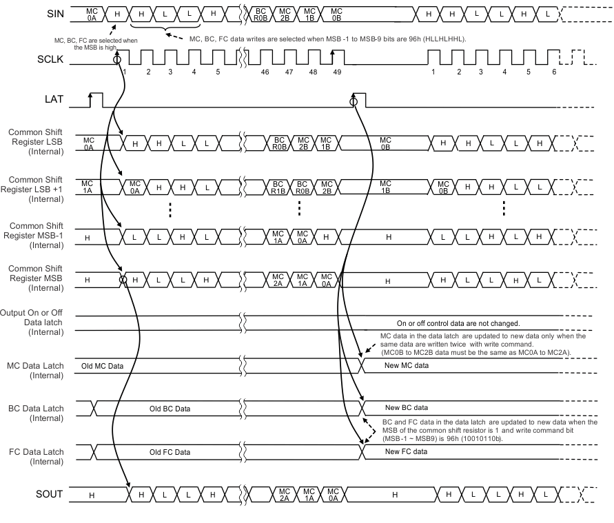 Figure 36. Maximum Current Control (MC), Global Brightness Control (BC), and Function Control (FC) Data Write Timing Diagram