JAJSFM7A May   2018  – June 2018 TLV7081

PRODUCTION DATA.  

  1. 特長
  2. アプリケーション
  3. 概要
    1.     Device Images
      1.      低電圧の検出
      2.      ISと電源電圧との関係
  4. 改訂履歴
  5. Pin Configuration and Functions
    1.     Pin Functions
  6. Specifications
    1. 6.1 Absolute Maximum Ratings
    2. 6.2 ESD Ratings
    3. 6.3 Recommended Operating Conditions
    4. 6.4 Thermal Information
    5. 6.5 Electrical Characteristics
    6. 6.6 Switching Characteristics
    7. 6.7 Timing Diagrams
    8. 6.8 Typical Characteristics
  7. Detailed Description
    1. 7.1 Overview
    2. 7.2 Functional Block Diagram
    3. 7.3 Feature Description
    4. 7.4 Device Functional Modes
      1. 7.4.1 Inputs
      2. 7.4.2 Internal Hysteresis
      3. 7.4.3 Output
  8. Application and Implementation
    1. 8.1 Application Information
    2. 8.2 Typical Applications
      1. 8.2.1 Nano-Power Battery Monitor
        1. 8.2.1.1 Design Requirements
        2. 8.2.1.2 Detailed Design Procedure
        3. 8.2.1.3 Application Curve
      2. 8.2.2 Battery Monitoring in Portable Electronics
  9. Layout
    1. 9.1 Layout Guidelines
    2. 9.2 Layout Example
  10. 10デバイスおよびドキュメントのサポート
    1. 10.1 ドキュメントのサポート
      1. 10.1.1 関連資料
    2. 10.2 ドキュメントの更新通知を受け取る方法
    3. 10.3 コミュニティ・リソース
    4. 10.4 Trademarks
    5. 10.5 Electrostatic Discharge Caution
    6. 10.6 Glossary
  11. 11メカニカル、パッケージ、および注文情報

パッケージ・オプション

メカニカル・データ(パッケージ|ピン)
サーマルパッド・メカニカル・データ
発注情報

Battery Monitoring in Portable Electronics

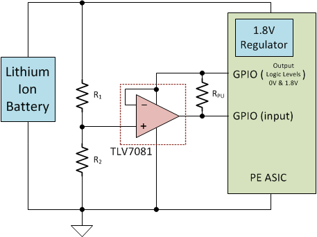
A recommended circuit diagram for monitoring a battery voltage in a personal electronic device is shown in Figure 23. In this diagram, the GPIO pin of an application specific integrated circuit (ASIC) serves as the supply voltage and the voltage reference for the TLV7081. Using a GPIO pin to power the TLV7081 is possible because of the low quiescent current of the TLV7081. In systems where power consumption needs to be further reduced, the GPIO pin can be used to power-cycle the TLV7081.
TLV7081 Voltage_MonA.gifFigure 23. Battery Monitor