JAJSFM7A May   2018  – June 2018 TLV7081

PRODUCTION DATA.  

  1. 特長
  2. アプリケーション
  3. 概要
    1.     Device Images
      1.      低電圧の検出
      2.      ISと電源電圧との関係
  4. 改訂履歴
  5. Pin Configuration and Functions
    1.     Pin Functions
  6. Specifications
    1. 6.1 Absolute Maximum Ratings
    2. 6.2 ESD Ratings
    3. 6.3 Recommended Operating Conditions
    4. 6.4 Thermal Information
    5. 6.5 Electrical Characteristics
    6. 6.6 Switching Characteristics
    7. 6.7 Timing Diagrams
    8. 6.8 Typical Characteristics
  7. Detailed Description
    1. 7.1 Overview
    2. 7.2 Functional Block Diagram
    3. 7.3 Feature Description
    4. 7.4 Device Functional Modes
      1. 7.4.1 Inputs
      2. 7.4.2 Internal Hysteresis
      3. 7.4.3 Output
  8. Application and Implementation
    1. 8.1 Application Information
    2. 8.2 Typical Applications
      1. 8.2.1 Nano-Power Battery Monitor
        1. 8.2.1.1 Design Requirements
        2. 8.2.1.2 Detailed Design Procedure
        3. 8.2.1.3 Application Curve
      2. 8.2.2 Battery Monitoring in Portable Electronics
  9. Layout
    1. 9.1 Layout Guidelines
    2. 9.2 Layout Example
  10. 10デバイスおよびドキュメントのサポート
    1. 10.1 ドキュメントのサポート
      1. 10.1.1 関連資料
    2. 10.2 ドキュメントの更新通知を受け取る方法
    3. 10.3 コミュニティ・リソース
    4. 10.4 Trademarks
    5. 10.5 Electrostatic Discharge Caution
    6. 10.6 Glossary
  11. 11メカニカル、パッケージ、および注文情報

パッケージ・オプション

メカニカル・データ(パッケージ|ピン)
サーマルパッド・メカニカル・データ
発注情報

Typical Characteristics

TA = 25°C, VS = 3.3 V, RPULL-UP = 4.99 kΩ, CL = 15 pF
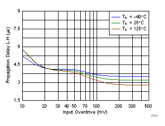
TLV7081 tPLH_vs_VOD_1.8V.gif
VS = 1.8 V
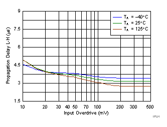
Figure 3. Propagation Delay (L-H) vs. Input Overdrive
TLV7081 tPLH_vs_VOD_3.3V.gif
VS = 3.3 V
Figure 5. Propagation Delay (L-H) vs. Input Overdrive
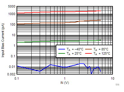
TLV7081 ibias_vcm_3.3v.gif
VS = 3.3 V
Figure 7. Input Bias Current vs. IN
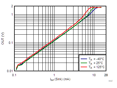
TLV7081 vout_iout_sink_1.8v.gif
VS = 1.8 V
Figure 9. Output Voltage Low vs. Output Sink Current
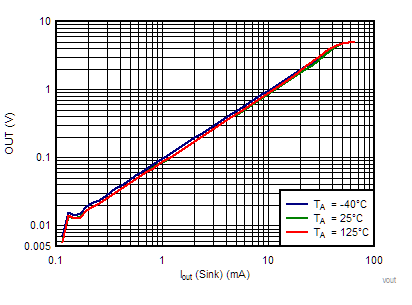
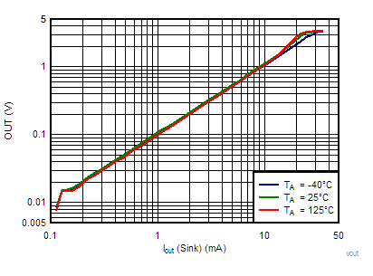
TLV7081 vout_iout_sink_5.0v.gif
VS = 5 V
Figure 11. Output Voltage Low vs. Output Sink Current
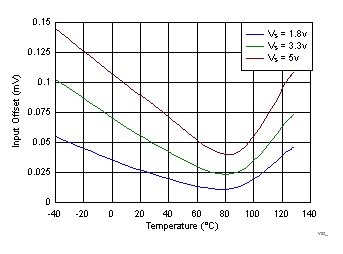
TLV7081 vio_ta.gif
Figure 13. Input Offset vs. Temperature
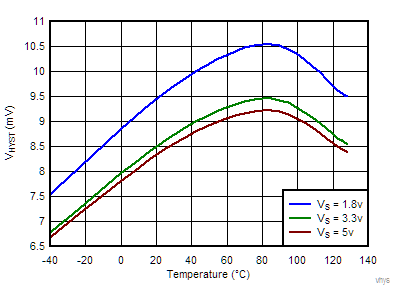
TLV7081 vhyst_ta.gif
Figure 15. Hysteresis vs. Temperature
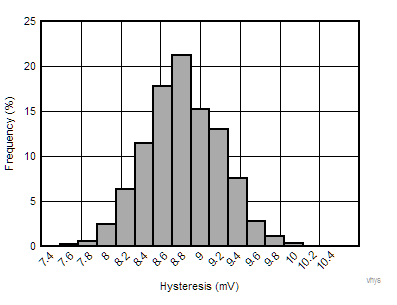
TLV7081 vhyst_historam.gif
Distribution Taken from 7,990 Comparators
Figure 17. Hysteresis Histogram
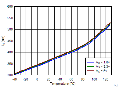
TLV7081 is_ta.gif
IN = (V+) - 0.1V (output low), No load.
Figure 19. Supply Current vs. Temperature
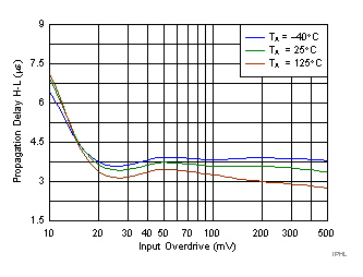
TLV7081 tPHL_vs_VOD_1.8V.gif
VS = 1.8 V
Figure 4. Propagation Delay (H-L) vs. Input Overdrive
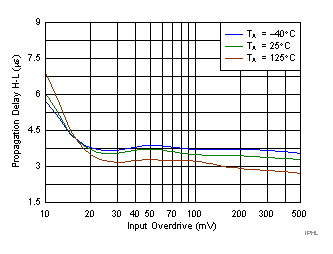
TLV7081 tPHL_vs_VOD_3.3V.gif
VS = 3.3 V
Figure 6. Propagation Delay (H-L) vs. Input Overdrive
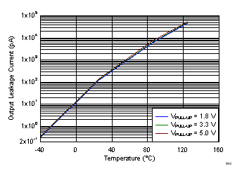
TLV7081 ileak_vs_temp.gif
Figure 8. Output Leakage Current vs. Temperature
TLV7081 vout_iout_sink_3.3v.gif
VS = 3.3 V
Figure 10. Output Voltage Low vs. Output Sink Current
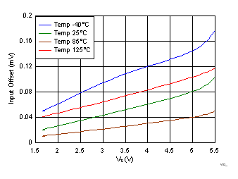
TLV7081 vio_vs.gif
Figure 12. Input Offset vs. VS
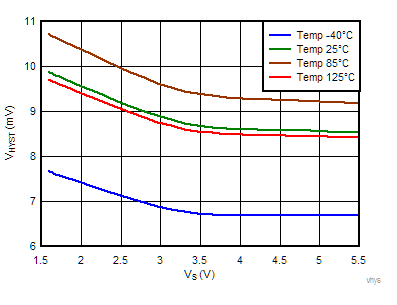
TLV7081 vhyst_vs.gif
Figure 14. Hysteresis vs VS
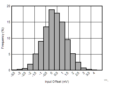
TLV7081 vos_historam.gif
Distribution Taken from 7,990 Comparators
Figure 16. Input Offset Histogram
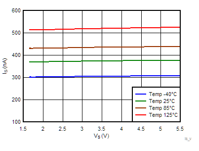
TLV7081 is_vs.gif
IN = (V+) - 0.1V (output low), No load.
Figure 18. Supply Current vs. VS