JAJSFM7A May   2018  – June 2018 TLV7081

PRODUCTION DATA.  

  1. 特長
  2. アプリケーション
  3. 概要
    1.     Device Images
      1.      低電圧の検出
      2.      ISと電源電圧との関係
  4. 改訂履歴
  5. Pin Configuration and Functions
    1.     Pin Functions
  6. Specifications
    1. 6.1 Absolute Maximum Ratings
    2. 6.2 ESD Ratings
    3. 6.3 Recommended Operating Conditions
    4. 6.4 Thermal Information
    5. 6.5 Electrical Characteristics
    6. 6.6 Switching Characteristics
    7. 6.7 Timing Diagrams
    8. 6.8 Typical Characteristics
  7. Detailed Description
    1. 7.1 Overview
    2. 7.2 Functional Block Diagram
    3. 7.3 Feature Description
    4. 7.4 Device Functional Modes
      1. 7.4.1 Inputs
      2. 7.4.2 Internal Hysteresis
      3. 7.4.3 Output
  8. Application and Implementation
    1. 8.1 Application Information
    2. 8.2 Typical Applications
      1. 8.2.1 Nano-Power Battery Monitor
        1. 8.2.1.1 Design Requirements
        2. 8.2.1.2 Detailed Design Procedure
        3. 8.2.1.3 Application Curve
      2. 8.2.2 Battery Monitoring in Portable Electronics
  9. Layout
    1. 9.1 Layout Guidelines
    2. 9.2 Layout Example
  10. 10デバイスおよびドキュメントのサポート
    1. 10.1 ドキュメントのサポート
      1. 10.1.1 関連資料
    2. 10.2 ドキュメントの更新通知を受け取る方法
    3. 10.3 コミュニティ・リソース
    4. 10.4 Trademarks
    5. 10.5 Electrostatic Discharge Caution
    6. 10.6 Glossary
  11. 11メカニカル、パッケージ、および注文情報

パッケージ・オプション

メカニカル・データ(パッケージ|ピン)
サーマルパッド・メカニカル・データ
発注情報

Internal Hysteresis

The device hysteresis transfer curve is shown in Figure 20. This curve is a function of three components: VTH, VOS, and VHYST:

  • VTH is the actual set voltage or threshold trip voltage.
  • VOS is the internal offset voltage between IN and V+. This voltage is added to VTH to form the actual trip point at which the comparator must respond to change output states.
  • VHYST is the internal hysteresis (or trip window) that is designed to reduce comparator sensitivity to noise
    (10 mV typical).
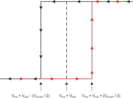
TLV7081 ai_hyst_transfer_bos694.gifFigure 20. Hysteresis Transfer Curve