JAJS427I July 2010 – October 2019 TPS63020 , TPS63021
PRODUCTION DATA.
- 1 特長
- 2 アプリケーション
- 3 概要
- 4 改訂履歴
- 5 概要 (続き)
- 6 Pin Configuration and Functions
- 7 Specifications
- 8 Detailed Description
- 9 Application and Implementation
- 10Power Supply Recommendations
- 11Layout
- 12デバイスおよびドキュメントのサポート
- 13メカニカル、パッケージ、および注文情報
パッケージ・オプション
メカニカル・データ(パッケージ|ピン)
- DSJ|14
サーマルパッド・メカニカル・データ
- DSJ|14
発注情報
8.4.3 Control Loop
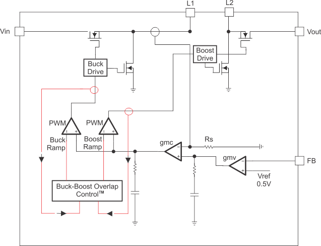
The controller circuit of the device is based on an average current mode topology. The average inductor current is regulated by a fast current regulator loop which is controlled by a voltage control loop. Figure 5 shows the control loop.
The non-inverting input of the transconductance amplifier, gmv, is assumed to be constant. The output of gmv defines the average inductor current. The inductor current is reconstructed by measuring the current through the high-side buck MOSFET. This current corresponds exactly to the inductor current in boost mode. In buck mode, the current is measured during the on-time of the same MOSFET. During the off-time, the current is reconstructed internally starting from the peak value at the end of the on-time cycle. The average current and the feedback from the error amplifier gmv forms the correction signal gmc. This correction signal is compared to the buck and the boost sawtooth ramp giving the PWM signal. Depending on which of the two ramps, the gmc output crosses either the buck or the boost stage is initiated. When the input voltage is close to the output voltage, one buck cycle is always followed by a boost cycle. In this condition, no more than three cycles in a row of the same mode are allowed. This control method in the buck-boost region ensures a robust control and the highest efficiency.
The buck-boost overlap control makes sure that the classical buck-boost function, which would cause two switches to be on every half a cycle, is avoided. Thanks to this block, whenever all switches becomes active during one clock cycle, the two ramps are shifted away from each other. On the other hand, when there is no switching activities because there is a gap between the ramps, the ramps are moved closer together. As a result, the number of classical buck-boost cycles or no switching is reduced to a minimum and high efficiency values has been achieved.
 Figure 5. Average Current Mode Control