JAJS427I July 2010 – October 2019 TPS63020 , TPS63021
PRODUCTION DATA.
- 1 特長
- 2 アプリケーション
- 3 概要
- 4 改訂履歴
- 5 概要 (続き)
- 6 Pin Configuration and Functions
- 7 Specifications
- 8 Detailed Description
- 9 Application and Implementation
- 10Power Supply Recommendations
- 11Layout
- 12デバイスおよびドキュメントのサポート
- 13メカニカル、パッケージ、および注文情報
パッケージ・オプション
メカニカル・データ(パッケージ|ピン)
- DSJ|14
サーマルパッド・メカニカル・データ
- DSJ|14
発注情報
8.4.4 Power Save Mode and Synchronization
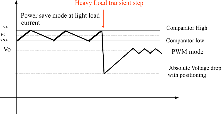
The PS/SYNC pin can be used to select different operation modes. Power save mode is used to improve efficiency at light load. To enable power save mode, PS/SYNC must be set low. If PS/SYNC is set low, then power save mode is entered when the average inductor current gets lower than about 100 mA. At this point, the converter operates with reduced switching frequency and with a minimum quiescent current to maintain high efficiency. See Figure 6 for detailed operation of the power save mode.
During the power save mode, the output voltage is monitored with a comparator by the threshold comp low and comp high. When the device enters power save mode, the converter stops operating and the output voltage drops. The slope of the output voltage depends on the load and the value of output capacitance. As the output voltage falls below the comp low threshold set to 2.5% typical above VOUT, the device ramps up the output voltage again, by starting operation using a programmed average inductor current higher than required by the current load condition. Operation can last one or several pulses. The converter continues these pulses until the comp high threshold, set to typically 3.5% above VOUT nominal, is reached and the average inductance current gets lower than about 100 mA. When the load increases above the minimum forced inductor current of about 100 mA, the device automatically switches to pulse width modulation (PWM) mode.
The power save mode can be disabled by programming high at the PS/SYNC. Connecting a clock signal at PS/SYNC forces the device to synchronize to the connected clock frequency.
Synchronization is done by a phase-locked loop (PLL), so synchronizing to lower and higher frequencies compared to the internal clock works without any issues. The PLL can also tolerate missing clock pulses without the converter malfunctioning. The PS/SYNC input supports standard logic thresholds.
 Figure 6. Power Save Mode Thresholds and Dynamic Voltage Positioning