JAJSNG4B January 2015 – January 2022 TPS65251-1 , TPS65251-2 , TPS65251-3
PRODUCTION DATA
- 1 特長
- 2 アプリケーション
- 3 概要
- 4 Revision History
- 5 Pin Configuration and Functions
- 6 Specifications
-
7 Detailed Description
- 7.1 Overview
- 7.2 Functional Block Diagram
- 7.3
Feature Description
- 7.3.1 Adjustable Switching Frequency
- 7.3.2 Synchronization
- 7.3.3 Out-of-Phase Operation
- 7.3.4 Delayed Start-Up
- 7.3.5 Soft-Start Time
- 7.3.6 Adjusting the Output Voltage
- 7.3.7 Input Capacitor
- 7.3.8 Bootstrap Capacitor
- 7.3.9 Error Amplifier
- 7.3.10 Slope Compensation
- 7.3.11 Power Good
- 7.3.12 3.3-V and 6.5-V LDO Regulators
- 7.3.13 Current Limit Protection
- 7.3.14 Overvoltage Transient Protection (OVP)
- 7.3.15 Thermal Shutdown
- 7.4 Device Functional Modes
-
8 Application and Implementation
- 8.1 Application Information
- 8.2
Typical Application
- 8.2.1 Design Requirements
- 8.2.2
Detailed Design Procedure
- 8.2.2.1 Loop Compensation Circuit
- 8.2.2.2 Selecting the Switching Frequency
- 8.2.2.3 Output Inductor Selection
- 8.2.2.4 Output Capacitor
- 8.2.2.5 Input Capacitor
- 8.2.2.6 Soft-Start Capacitor
- 8.2.2.7 Bootstrap Capacitor Selection
- 8.2.2.8 Adjustable Current Limiting Resistor Selection
- 8.2.2.9 Output Voltage and Feedback Resistors Selection
- 8.2.2.10 Compensation
- 8.2.2.11 3.3-V and 6.5-V LDO Regulators
- 8.2.3 Application Curves
- 9 Power Supply Recommendations
- 10Layout
- 11Device and Documentation Support
- 12Mechanical, Packaging, and Orderable Information
パッケージ・オプション
メカニカル・データ(パッケージ|ピン)
- RHA|40
サーマルパッド・メカニカル・データ
- RHA|40
発注情報
8.2.2.1 Loop Compensation Circuit
A typical compensation circuit could be type II (Rc and Cc) to have a phase margin between 60° and 90°, or type III (Rc, Cc and Cff) to improve the converter transient response. CRoll adds a high frequency pole to attenuate high-frequency noise when needed. It may also prevent noise coupling from other rails if there is possibility of cross coupling in between rails when layout is very compact.
 Figure 8-2 Loop Compensation
To calculate the external compensation components use Table 8-1:
Table 8-1 Design Guideline for the Loop Compensation
| TYPE II CIRCUIT | TYPE III CIRCUIT | |
|---|---|---|
| Select switching frequency that is appropriate for application depending on L, C sizes, output ripple, EMI concerns and etc. Switching frequencies between 500 kHz and 1 MHz give best trade off between performance and cost. When using smaller L and Cs, switching frequency can be increased. To optimize efficiency, switching frequency can be lowered. | Type III circuit recommended for switching frequencies higher than 500 kHz. | |
| Select cross over frequency (fc) to be less than 1/5 to 1/10 of switching frequency. | Suggested fc = fs/10 | Suggested fc = fs/10 |
| Set and calculate Rc. | Equation 6. 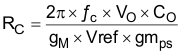 | Equation 7. 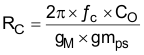 |
| Calculate Cc by placing a compensation zero at or before the converter dominant pole
Equation 8. 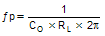 | Equation 9. 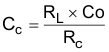 | Equation 10. |
| Add CRoll if needed to remove large signal coupling to high impedance COMP node. Make sure that
Equation 11. is at least twice the cross over frequency.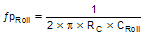 | Equation 12. 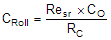 | Equation 13. |
| Calculate Cff compensation zero at low frequency to boost the phase margin at the crossover frequency. Make sure that the zero frequency (fzff is smaller than soft-start equivalent frequency (1/Tss). | NA | Equation 14. 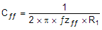 |