JAJSNG4B January 2015 – January 2022 TPS65251-1 , TPS65251-2 , TPS65251-3
PRODUCTION DATA
- 1 特長
- 2 アプリケーション
- 3 概要
- 4 Revision History
- 5 Pin Configuration and Functions
- 6 Specifications
-
7 Detailed Description
- 7.1 Overview
- 7.2 Functional Block Diagram
- 7.3
Feature Description
- 7.3.1 Adjustable Switching Frequency
- 7.3.2 Synchronization
- 7.3.3 Out-of-Phase Operation
- 7.3.4 Delayed Start-Up
- 7.3.5 Soft-Start Time
- 7.3.6 Adjusting the Output Voltage
- 7.3.7 Input Capacitor
- 7.3.8 Bootstrap Capacitor
- 7.3.9 Error Amplifier
- 7.3.10 Slope Compensation
- 7.3.11 Power Good
- 7.3.12 3.3-V and 6.5-V LDO Regulators
- 7.3.13 Current Limit Protection
- 7.3.14 Overvoltage Transient Protection (OVP)
- 7.3.15 Thermal Shutdown
- 7.4 Device Functional Modes
-
8 Application and Implementation
- 8.1 Application Information
- 8.2
Typical Application
- 8.2.1 Design Requirements
- 8.2.2
Detailed Design Procedure
- 8.2.2.1 Loop Compensation Circuit
- 8.2.2.2 Selecting the Switching Frequency
- 8.2.2.3 Output Inductor Selection
- 8.2.2.4 Output Capacitor
- 8.2.2.5 Input Capacitor
- 8.2.2.6 Soft-Start Capacitor
- 8.2.2.7 Bootstrap Capacitor Selection
- 8.2.2.8 Adjustable Current Limiting Resistor Selection
- 8.2.2.9 Output Voltage and Feedback Resistors Selection
- 8.2.2.10 Compensation
- 8.2.2.11 3.3-V and 6.5-V LDO Regulators
- 8.2.3 Application Curves
- 9 Power Supply Recommendations
- 10Layout
- 11Device and Documentation Support
- 12Mechanical, Packaging, and Orderable Information
パッケージ・オプション
メカニカル・データ(パッケージ|ピン)
- RHA|40
サーマルパッド・メカニカル・データ
- RHA|40
発注情報
8.2.2.4 Output Capacitor
There are two primary considerations for selecting the value of the output capacitor. The output capacitors are selected to meet load transient and output ripple’s requirements.
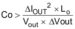
Equation 19 gives the minimum output capacitance to meet the transient specification. For this example,
LO = 4.7 µH, ΔIOUT = 1.5 A – 0.75 A = 0.75 A and ΔVOUT = 120 mV. Using these numbers gives a minimum capacitance of 18 µF. A standard 22-µF ceramic capacitor is chose in the design.
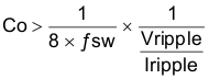
Equation 20 calculates the minimum output capacitance needed to meet the output voltage ripple specification. Where fsw is the switching frequency, VRIPPLE is the maximum allowable output voltage ripple, and IRIPPLE is the inductor ripple current. In this case, the maximum output voltage ripple is 30 mV. From Equation 16, the output current ripple is 0.46 A. From Equation 20, the minimum output capacitance meeting the output voltage ripple requirement is 1.74 µF.
Additional capacitance de-rating for aging, temperature and DC bias should influence this minimum value. For this example, one 22-µF, 6.3-V X7R ceramic capacitor with 3 mΩ of ESR will be used.