JAJSNG4B January 2015 – January 2022 TPS65251-1 , TPS65251-2 , TPS65251-3
PRODUCTION DATA
- 1 特長
- 2 アプリケーション
- 3 概要
- 4 Revision History
- 5 Pin Configuration and Functions
- 6 Specifications
-
7 Detailed Description
- 7.1 Overview
- 7.2 Functional Block Diagram
- 7.3
Feature Description
- 7.3.1 Adjustable Switching Frequency
- 7.3.2 Synchronization
- 7.3.3 Out-of-Phase Operation
- 7.3.4 Delayed Start-Up
- 7.3.5 Soft-Start Time
- 7.3.6 Adjusting the Output Voltage
- 7.3.7 Input Capacitor
- 7.3.8 Bootstrap Capacitor
- 7.3.9 Error Amplifier
- 7.3.10 Slope Compensation
- 7.3.11 Power Good
- 7.3.12 3.3-V and 6.5-V LDO Regulators
- 7.3.13 Current Limit Protection
- 7.3.14 Overvoltage Transient Protection (OVP)
- 7.3.15 Thermal Shutdown
- 7.4 Device Functional Modes
-
8 Application and Implementation
- 8.1 Application Information
- 8.2
Typical Application
- 8.2.1 Design Requirements
- 8.2.2
Detailed Design Procedure
- 8.2.2.1 Loop Compensation Circuit
- 8.2.2.2 Selecting the Switching Frequency
- 8.2.2.3 Output Inductor Selection
- 8.2.2.4 Output Capacitor
- 8.2.2.5 Input Capacitor
- 8.2.2.6 Soft-Start Capacitor
- 8.2.2.7 Bootstrap Capacitor Selection
- 8.2.2.8 Adjustable Current Limiting Resistor Selection
- 8.2.2.9 Output Voltage and Feedback Resistors Selection
- 8.2.2.10 Compensation
- 8.2.2.11 3.3-V and 6.5-V LDO Regulators
- 8.2.3 Application Curves
- 9 Power Supply Recommendations
- 10Layout
- 11Device and Documentation Support
- 12Mechanical, Packaging, and Orderable Information
パッケージ・オプション
メカニカル・データ(パッケージ|ピン)
- RHA|40
サーマルパッド・メカニカル・データ
- RHA|40
発注情報
5 Pin Configuration and Functions
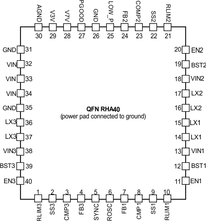
Table 5-1 Pin Functions
| PIN | I/O | DESCRIPTION | |
|---|---|---|---|
| NAME | NO. | ||
| RLIM3 | 1 | I | Current limit setting for Buck 3. Fit a resistor from this pin to ground to set the peak current limit on the output inductor. |
| SS3 | 2 | I | Soft-start pin for Buck 3. Fit a small ceramic capacitor to this pin to set the converter soft-start time. |
| COMP3 | 3 | O | Compensation for Buck 3. Fit a series RC circuit to this pin to complete the compensation circuit of this converter. |
| FB3 | 4 | I | Feedback input for Buck 3. Connect a divider set to 0.8 V from the output of the converter to ground. |
| SYNC | 5 | I | Synchronous clock input. If there is a sync clock in the system, connect to the pin. When not used, connect to GND. |
| ROSC | 6 | I | Oscillator set. This resistor sets the frequency of the internal autonomous clock. If external synchronization is used, the resistor should be fitted and set to about 70% of external clock frequency. |
| FB1 | 7 | I | Feedback pin for Buck 1. Connect a divider set to 0.8 V from the output of the converter to ground. |
| COMP1 | 8 | O | Compensation pin for Buck 1. Fit a series RC circuit to this pin to complete the compensation circuit of this converter. |
| SS1 | 9 | I | Soft-start pin for Buck 1. Fit a small ceramic capacitor to this pin to set the converter soft-start time. |
| RLIM1 | 10 | I | Current limit setting pin for Buck 1. Fit a resistor from this pin to ground to set the peak current limit on the output inductor. |
| EN1 | 11 | I | Enable pin for Buck 1. A low-level signal on this pin disables it. If pin is left open, a weak internal pull-up to V3V allows for automatic enable. For a delayed start-up, add a small ceramic capacitor from this pin to ground. |
| BST1 | 12 | I | Bootstrap capacitor for Buck 1. Fit a 47-nF ceramic capacitor from this pin to the switching node. |
| VIN1 | 13 | I | Input supply for Buck 1. Fit a 10-µF ceramic capacitor close to this pin. |
| LX1 | 14 | O | Switching node for Buck 1 |
| 15 | |||
| LX2 | 16 | O | Switching node for Buck 2 |
| 17 | |||
| VIN2 | 18 | I | Input supply for Buck 2. Fit a 10-µF ceramic capacitor close to this pin. |
| BST2 | 19 | I | Bootstrap capacitor for Buck 2. Fit a 47-nF ceramic capacitor from this pin to the switching node. |
| EN2 | 20 | I | Enable pin for Buck 2. A low-level signal on this pin disables it. If pin is left open, a weak internal pull-up to V3V allows for automatic enable. For a delayed start-up, add a small ceramic capacitor from this pin to ground. |
| RLIM2 | 21 | I | Current limit setting for Buck 2. Fit a resistor from this pin to ground to set the peak current limit on the output inductor. |
| SS2 | 22 | I | Soft-start pin for Buck 2. Fit a small ceramic capacitor to this pin to set the converter soft-start time. |
| COMP2 | 23 | O | Compensation pin for Buck 2. Fit a series RC circuit to this pin to complete the compensation circuit of this converter |
| FB2 | 24 | I | Feedback input for Buck 2. Connect a divider set to 0.8 V from the output of the converter to ground. |
| LOW_P | 25 | I | Low-power operation mode (active-high) input for TPS65251 |
| GND | 26 | Ground pin | |
| PGOOD | 27 | O | Power good. Open-drain output asserted after all converters are sequenced and within regulation. Polarity is factory selectable (active-high default). |
| V7V | 28 | O | Internal supply. Connect a 10-μF ceramic capacitor from this pin to ground. |
| V3V | 29 | O | Internal supply. Connect a 3.3- to 10-μF ceramic capacitor from this pin to ground. |
| AGND | 30 | Analog ground. Connect all GND pins and the power pad together. | |
| GND | 31 | Ground pin | |
| VIN | 32 | I | Input supply |
| 33 | |||
| 34 | |||
| GND | 35 | Ground pin | |
| LX3 | 36 | O | Switching node for Buck 3 |
| 37 | |||
| VIN3 | 38 | Input supply for Buck 3. Fit a 10-µF ceramic capacitor close to this pin. | |
| BST3 | 39 | I | Bootstrap capacitor for Buck 3. Fit a 47-nF ceramic capacitor from this pin to the switching node. |
| EN3 | 40 | I | Enable pin for Buck 3. A low-level signal on this pin disables it. If pin is left open, a weak internal pull-up to V3V allows for automatic enable. For a delayed start-up, add a small ceramic capacitor from this pin to ground. |
| PAD | — | — | Power pad. Connect to ground. |