JAJU528B August 2022 – January 2023 OPA388-Q1
- 概要
- リソース
- 特長
- アプリケーション
- 5
- 1System Description
- 2System Overview
- 3Hardware, Testing Requirements, and Test Results
- 4Design Files
- 5Software Files
- 6Related Documentation
- 7Trademarks
- 8Revision History
3.2.2.3 Isolation Error at HV Negative
An error condition is created by connecting the HV negative line to chassis ground. To understand the behavior of error conditions, measurements were performed at different battery voltages.
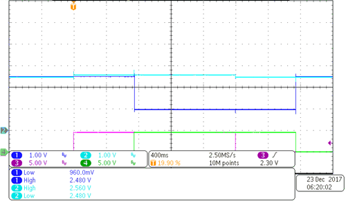
 Figure 3-15 HV Negative Error 400 V at No Resistance Figure 3-15 HV Negative Error 400 V at No Resistance | No resistance from HV negative line to chassis ground |
| CH1: ISO_POS CH2: ISO_NEG CH3: RELAY_NEG CH4: RELAY_POS | |
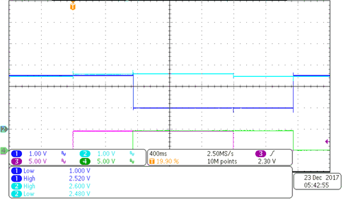
 Figure 3-16 HV Negative Error 400 V at 100-kΩ Resistance Figure 3-16 HV Negative Error 400 V at 100-kΩ Resistance | 100-kΩ resistance from positive line to chassis ground |
| CH1: ISO_POS CH2: ISO_NEG CH3: RELAY_NEG CH4: RELAY_POS | |
Table 3-3 Measurements at HV Negative Error
| HV BATTERY VOLTAGE (SUPPLIED AND MEASURED) | MEASURED REFERENCE VOLTAGE | MEASURED PEAK ISO_POS VOLTAGE | MEASURED PEAK ISO_NEG VOLTAGE |
|---|---|---|---|
| 100.006 | 2.505 | 2.191 | 2.61 |
| 150.008 | 2.504 | 1.982 | 2.61 |
| 200.003 | 2.504 | 1.774 | 2.61 |
| 250.004 | 2.504 | 1.565 | 2.61 |
| 300.004 | 2.504 | 1.357 | 2.61 |
| 350.004 | 2.504 | 1.148 | 2.61 |
| 400.006 | 2.504 | 0.939 | 2.61 |
| 450.007 | 2.504 | 0.731 | 2.61 |
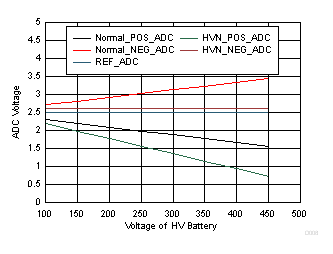
Figure 3-17 shows the deviations of HV POS and HV NEG ADC voltages from the normal conditions. HV NEG ADC is slightly above the reference voltage and constant when U7 (negative relay) is closed. This behavior is observable only when the HV negative line is low ohmic or short to chassis ground.
 Figure 3-17 Behavior for HV Negative Isolation Error