JAJU858 December   2022


  1.   概要
  2.   リソース
  3.   特長
  4.   アプリケーション
  5.   5
  6. 1System Description
    1.     7
    2. 1.1 EV Charging Station Challenges
      1. 1.1.1 SAE J1772 or Equivalent Standard Compliant EV Charging Stations
      2. 1.1.2 AC and DC Leakage, Residual Current Detection (RCD)
      3. 1.1.3 Efficient Relay and Contactor Drive
      4. 1.1.4 Contact Weld Detection
    3. 1.2 Key System Specifications
  7. 2System Overview
    1. 2.1 Block Diagram
    2. 2.2 Design Considerations
      1. 2.2.1 Isolated AC/DC Power Supply Design
        1. 2.2.1.1  Input Bulk Capacitance and Minimum Bulk Voltage
        2. 2.2.1.2  Transformer Turns-Ratio, Primary Inductance, and Primary Peak Current
        3. 2.2.1.3  Transformer Parameter Calculations: Primary and Secondary RMS Currents
        4. 2.2.1.4  Main Switching Power MOSFET Selection
        5. 2.2.1.5  Rectifying Diode Selection
        6. 2.2.1.6  Output Capacitor Selection
        7. 2.2.1.7  Capacitance on VDD Pin
        8. 2.2.1.8  Open-loop Voltage Regulation Versus Pin Resistor Divider, Line Compensation Resistor
        9. 2.2.1.9  Feedback Elements
        10. 2.2.1.10 Backup Power Supply
        11. 2.2.1.11 Supercapacitor Selection
        12. 2.2.1.12 Supercapacitor Charger Design
      2. 2.2.2 Control Pilot Signal Interface
        1. 2.2.2.1 J1772 Duty Cycle
          1. 2.2.2.1.1 Control Pilot Signal States
          2. 2.2.2.1.2 Control Pilot Signal Circuit
      3. 2.2.3 Relay Drive and Weld Detect
      4. 2.2.4 Residual Current Detection
        1. 2.2.4.1 Auto-Oscillation Circuit
          1.        37
        2. 2.2.4.2 DRV8220 H-Bridge
        3. 2.2.4.3 Saturation Detection Circuit
        4. 2.2.4.4 H-Bridge Controlled by DFF
        5. 2.2.4.5 Filter Stage
        6. 2.2.4.6 Differential to Single-Ended Converter
        7. 2.2.4.7 Low-Pass Filter
        8. 2.2.4.8 Full-Wave Rectifier
        9. 2.2.4.9 MCU Selection
    3. 2.3 Highlighted Products
      1. 2.3.1  UCC28742
      2. 2.3.2  TLV1805
      3. 2.3.3  DRV8220
      4. 2.3.4  ISO1212
      5. 2.3.5  ADC122S051
      6. 2.3.6  TPS7A39
      7. 2.3.7  TPS7A20
      8. 2.3.8  ATL431
      9. 2.3.9  TL431
      10. 2.3.10 TPS563210A
      11. 2.3.11 TPS55330
      12. 2.3.12 TPS259470
      13. 2.3.13 TL7705A
  8. 3Hardware, Testing Requirements, and Test Results
    1. 3.1 Hardware Requirements
    2. 3.2 Test Requirements
      1. 3.2.1 Power Supply Test Setup
      2. 3.2.2 Weld Detect Test Setup
    3. 3.3 Test Results
      1. 3.3.1 Isolated AC/DC Power Supply Based on UCC28742
        1. 3.3.1.1 Efficiency and Output Voltage Cross Regulation
        2. 3.3.1.2 Efficiency and Output Voltage Regulation of TPS563210
        3. 3.3.1.3 Output Voltage Ripple Waveforms
        4. 3.3.1.4 Start, Shutdown, Backup Power, and Transient Response Waveforms
        5. 3.3.1.5 Thermal Performance
      2. 3.3.2 TLV1805-Based Control Pilot Interface
        1. 3.3.2.1 TLV1805 Output Rise and Fall Time
        2. 3.3.2.2 Control Pilot Signal Voltage Accuracy in Different States
      3. 3.3.3 DRV8220-Based Relay and Plug Lock Drive
      4. 3.3.4 ISO1212-Based Isolated Line Voltage Sensing
  9. 4Design and Documentation Support
    1. 4.1 Design Files
      1. 4.1.1 Schematics
      2. 4.1.2 Bill of Materials
    2. 4.2 Documentation Support
    3. 4.3 サポート・リソース
    4. 4.4 Trademarks
  10. 5About the Author
Control Pilot Signal Circuit

The pilot signal is required to travel down several meters of cable and through a load resistance. The pilot signal is also a bipolar ±12-V signal, which requires special consideration. To accommodate these parameters, an amplifier with a wide input range and reasonable power output is selected. The TLV1805 device has a voltage rating of ±18 V and a current rating of 475 mA, making the device a good match for the application. In addition, while most EVSEs do not require an automotive qualification, a Q1-rated variant of the TLV1805-Q1 device exists, if this feature is desired.

The amplification circuit is a simple rail-to-rail output configuration of the TLV1805 device, with the MCU I/O driving the positive input. The output of the pilot amplifier is also fed into a simple voltage divider so that the MCU can measure the voltage during operation and detect the load resistance of the vehicle. Figure 2-3 shows the full schematic of this subsystem.
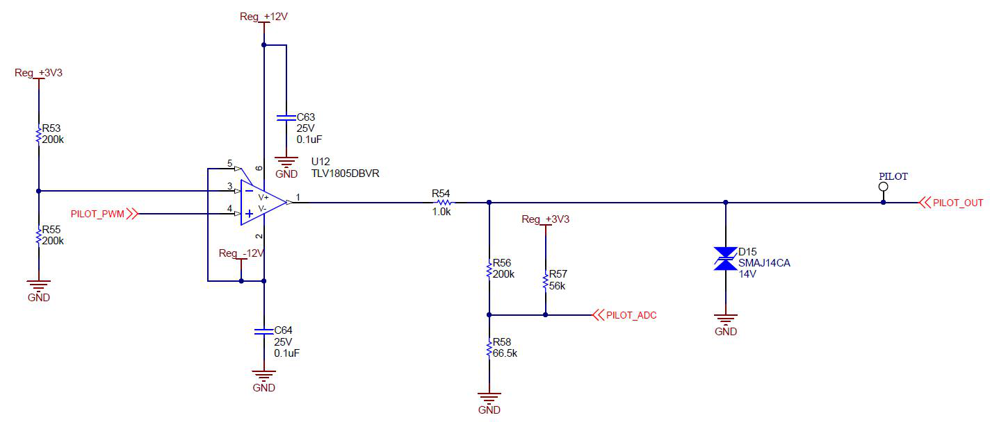
GUID-7DE8175D-DF2B-483E-9D94-74F2F8561FAF-low.pngFigure 2-3 Control Pilot Signal Generator Circuit

To validate the architecture, the design was tested in the TINA-TI™ software from TI, which is a spice-based simulation tool.