SLLU149E June 2011 – February 2016 TUSB7320 , TUSB7340
- TUSB73x0 Board Design and Layout Guidelines
- 1 Typical System Implementation
- 2 Power
- 3 Device Reset
- 4 General High Speed Layout Guidelines
- 5 USB Connection
- 6 Package and Breakout
- 7 PCI Express Connection
- 8 Wake from S3
- 9 Device Input Clock
- 10JTAG Interface
- 11Differential Pair ESD Protection
- 12SuperSpeed Redriver
- 13SMI Pin Implementation
- 14Schematics
- Revision History
5.2 Internal Chip Trace Length Mismatch
Routing of the differential pair on the PCB will need to account for length mismatch in the package. This is due to offset pin and the associated bond wire mismatch.
Table 5-1 Length Mismatch
| NetName | Bondwire Length (mil) | Difference (mil) |
|---|---|---|
| USB_SSTXN_DN1 | 96 | 20 |
| USB_SSTXP_DN1 | 116 | |
| USB_SSRXN_DN1 | 91 | 20 |
| USB_SSRXP_DN1 | 111 | |
| USB_DM_DN1 | 83 | 22 |
| USB_DP_DN1 | 105 | |
| USB_SSTXP_DN2 | 104 | 31 |
| USB_SSTXN_DN2 | 73 | |
| USB_SSRXP_DN2 | 67 | 27 |
| USB_SSRXN_DN2 | 94 | |
| USB_DM_DN2 | 127 | 34 |
| USB_DP_DN2 | 93 | |
| USB_SSTXP_DN3 | 73 | 30 |
| USB_SSTXN_DN3 | 103 | |
| USB_SSRXP_DN3 | 82 | 31 |
| USB_SSRXN_DN3 | 113 | |
| USB_DP_DN3 | 104 | 34 |
| USB_DM_DN3 | 138 | |
| USB_SSTXP_DN4 | 58 | 24 |
| USB_SSTXN_DN4 | 82 | |
| USB_SSRXP_DN4 | 58 | 22 |
| USB_SSRXN_DN4 | 80 | |
| USB_DM_DN4 | 86 | 26 |
| USB_DP_DN4 | 60 |
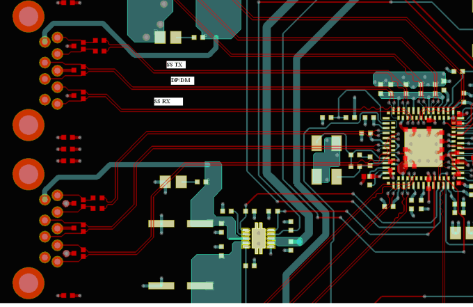
 Figure 5-1 USB3 and USB2 Signals from the USB Connector to the Device
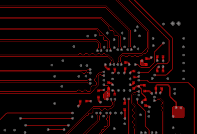
 Figure 5-2 shows length matching at the device. Length matching must be done at the device side, not at the connector.
 Figure 5-2 Length Matching