SLLU149E June 2011 – February 2016 TUSB7320 , TUSB7340
- TUSB73x0 Board Design and Layout Guidelines
- 1 Typical System Implementation
- 2 Power
- 3 Device Reset
- 4 General High Speed Layout Guidelines
- 5 USB Connection
- 6 Package and Breakout
- 7 PCI Express Connection
- 8 Wake from S3
- 9 Device Input Clock
- 10JTAG Interface
- 11Differential Pair ESD Protection
- 12SuperSpeed Redriver
- 13SMI Pin Implementation
- 14Schematics
- Revision History
9.1 Overview
The TUSB73x0 supports an external oscillator source or a crystal unit. If a clock is provided to XI instead of a crystal, it must be a 1.8-V clock source, XO should be left open and VSSOSC is connected to the PCB ground plane. Otherwise, if a crystal is used, the connection needs to follow the guidelines below.
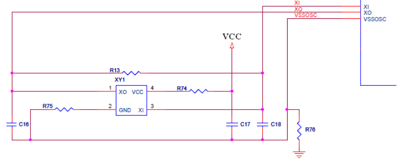
In Figure 9-1, XY1 is a dual crystal/oscillator footprint. To use a crystal only populate R13, C16, and C18. To use an oscillator only populate C17, R74, R75, and R76.
 Figure 9-1 Dual Crystal/Oscillator Footprint
 Since XI and XO are coupled to other leads and supplies on the PCB, it is important to keep them as short as possible and away from any switching leads. It is also recommended to minimize the capacitance between XI and XO. This can be accomplished by connecting the VSSOSC lead to the two external capacitors CL1 and CL2 and shielding them with the clean ground lines. The VSSOSC should not be connected to PCB ground if using a crystal.
Load capacitance (Cload) of the crystal varying with the crystal vendors is the total capacitance value of the entire oscillation circuit system as seen from the crystal. It includes two external capacitors CL1 and CL2. The trace length between the decoupling capacitors and the corresponding power pins on the TUSB73x0 needs to be minimized. It is also recommended that the trace length from the capacitor pad to the power or ground plane be minimized.
See the TUSB73x0 Data Sheet for input clock parameters.