SLOA198A September 2014 – December 2021 DRV2665 , DRV2667 , DRV2700 , DRV8662
- Trademarks
- 1 Boost Converter Basics
- 2 DRV8662, DRV2700, DRV2665, and DRV2667 Boost Converter
- 3 Configuring the Boost Converter
- 4 Boost Converter Output Voltage
- 5 Calculating the Load Current
- 6 Selecting an Inductor
- 7 Calculate the Maximum Boost Current
- 8 Output Capacitor Selection
- 9 Input Capacitor Selection
- 10PCB Layout
- 11Examples
- 12Revision History
4 Boost Converter Output Voltage
Set the boost converter based on the rated or maximum voltage required by the load. Add an additional 5 V to provide headroom when using the amplifier. Use Equation 1 to calculate the boost voltage.
Equation 1. VBOOST =
VPEAK + 5 V
| Symbol | Description | Value | Unit |
|---|---|---|---|
| VBOOST | Boost output voltage | - | V |
| VPEAK | Peak amplifier output voltage | - | V |
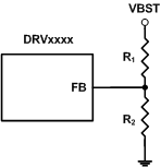
The boost output voltage is programmed by two external resistors shown in the following diagram:
The boost feedback resistors can be calculated using equation Equation 2:
Equation 2. 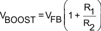
Note:
Ensure that the sum of R1 and R2 is greater than 400 kΩ to prevent large leakage currents due to high voltages on VBOOST.