SLOA198A September 2014 – December 2021 DRV2665 , DRV2667 , DRV2700 , DRV8662
- Trademarks
- 1 Boost Converter Basics
- 2 DRV8662, DRV2700, DRV2665, and DRV2667 Boost Converter
- 3 Configuring the Boost Converter
- 4 Boost Converter Output Voltage
- 5 Calculating the Load Current
- 6 Selecting an Inductor
- 7 Calculate the Maximum Boost Current
- 8 Output Capacitor Selection
- 9 Input Capacitor Selection
- 10PCB Layout
- 11Examples
- 12Revision History
8 Output Capacitor Selection
The output capacitor is important for decreasing output voltage ripple and reducing the effects of load transients on the boost voltage. The boost output voltage can be configured from 20 V up to 105 V, so the boost output capacitor must have a voltage rating equivalent to the boost output voltage or higher. A 250-V rated, 100-nF capacitor of X5R or X7R type is recommended for a boost converter voltage of 105 V. The selected capacitor should have a minimum working capacitance of 50 nF.
To estimate the absolute minimum capacitance required, use Equation 10. Typically the DRVxxxx devices operate with a switching frequency between 800 kHz to 1 MHz. To include additional margin for the device loop response, it is best to use one-sixth of the switching frequency (ƒ).
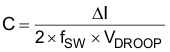
| Symbol | Description | Value | Unit |
|---|---|---|---|
| DELTA I | Boost transient current | 0 – 0.070 | mA |
| VDROOP | Maximum boost output voltage droop | – | V |
| fSW | Boost switching frequency | Typically 800kHz-1MHz | Hz |
| C | Output capacitor | – | F |
| Tip |
| A guideline for ceramic capacitors: the de-rated capacitance is approximately equal to the rated capacitance multiplied by one minus the applied voltage over the rated voltage. |
| Cde-rated = Crated (1 – Vapplied/Vrated) |
| For example, when 50 V is applied to a 100-V rated capacitor, the capacitance will decrease by about 50%. Most capacitor vendors provide a capacitance versus voltage curve for reference. |