SLOA198A September 2014 – December 2021 DRV2665 , DRV2667 , DRV2700 , DRV8662
- Trademarks
- 1 Boost Converter Basics
- 2 DRV8662, DRV2700, DRV2665, and DRV2667 Boost Converter
- 3 Configuring the Boost Converter
- 4 Boost Converter Output Voltage
- 5 Calculating the Load Current
- 6 Selecting an Inductor
- 7 Calculate the Maximum Boost Current
- 8 Output Capacitor Selection
- 9 Input Capacitor Selection
- 10PCB Layout
- 11Examples
- 12Revision History
6.1 Inductance Rating
The inductance sets the maximum switching frequency of the boost converter. The general trade off with inductances between 3.3 µH and 22 µH are:
- Larger inductances (10 µH or greater)
- Advantage: Cause the boost converter to run at a lower switching frequency meaning less switching losses.
- Disadvantage: Larger values typically have higher series resistance and lower saturation currents, requiring physically larger inductors.
- Smaller inductances (Less than 10 µH)
- Advantage: Typically have higher saturation currents and are a better choice for maximizing output current of the boost converter per inductor area.
- Disadvantage: Higher switching frequencies can lead to more losses. Switching losses are not a major concern in most applications, but if thermal dissipation is a concern because of a small PCB or extreme temperatures, then consider using a larger inductance.
The approximate switching frequency can be calculated using Equation 4:
Equation 4. 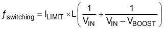
| Symbol | Description | Value | Unit |
|---|---|---|---|
| fswitching | DRVxxx switching frequency | – | Hz |
| VIN | Minimum VDD voltage applied to the DRVxxxx | – | V |
| VBOOST | Maximum boost output voltage | – | V |
| ILIMIT | Current limit set by the DRVxxxx REXT resistor | – | Ap |
| Tip |
| Smaller inductances (3.3 – 4.7 µH) are often preferred in space-constrained applications because of their size, higher saturation current, and ability to deliver more charge to the load. |