SLUAAU1 January 2024 BQ25700A , BQ25708 , BQ25710 , BQ25713 , BQ25720 , BQ25723 , BQ25730 , BQ25731
- 1
- Abstract
- Trademarks
- 1Introduction
-
2Layout Guidelines
- 2.1 PCB Stack-Up (4 Layers)
- 2.2 Identifying Critical Circuit Paths
- 2.3 Input and Output Loop Placements Considering Noise, Efficiency, and Thermal Performance
- 2.4 Kelvin Sensing Circuit for Current Sense to Achieve High Accuracy
- 2.5 Small Capacitors Placements Considering Noise
- 2.6 Separating AGND and PGND
- 3References
2.5 Small Capacitors Placements Considering Noise
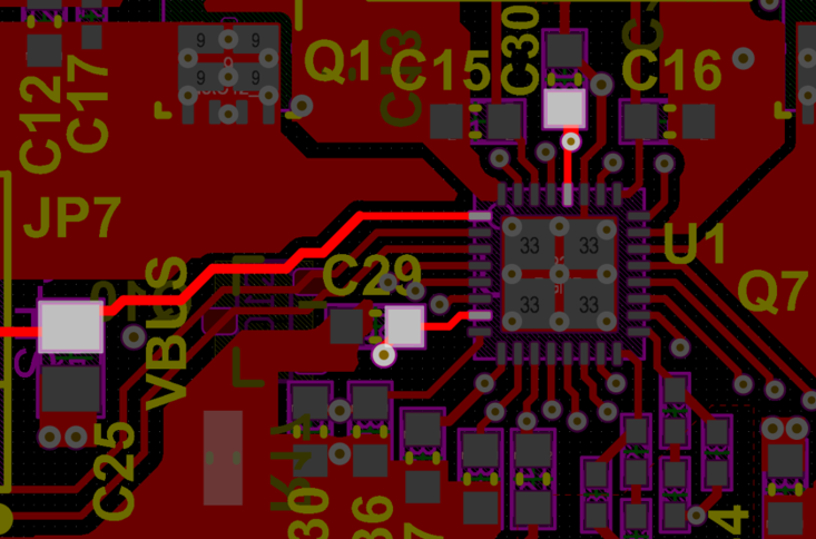
Place REGN capacitor(C30), VBUS capacitor(C25), VDDA capacitor(C29) close to IC as shown in Figure 2-6. Use AGND for VBUS, VDDA capacitors and use PGND for REGN capacitor since REGN pin out is for power stage gate drive. Since REGN capacitor provides a low impedance path for the driver circuits in BQ25710, put REGN capacitor close to the IC to maintain the lowest impedance source for the fast di/dt required for IC’s FET drivers.
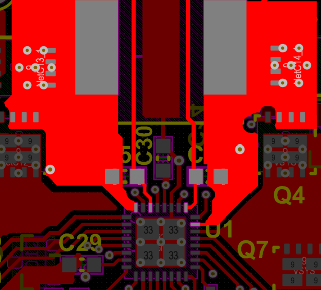
Place high-side FET bootstrap circuit capacitors close to IC and on the same layer of PCB. As shown in Figure 2-7, capacitors on SW1/2 nodes are recommended to use wide copper polygon to connect to power stage and capacitors on BTST1/2 nodes are recommended to use at least 8mil trace to connected to BTST1/2 pins to reduce line parasitic inductance. Another R/C for signal pins must be placed close to the IC far away from high frequency noise. Add ground vias close to R/C to connect the ground of signal to ground plane.
 Figure 2-6 Capacitors Placement for VBUS,
VDDA, REGN
 Figure 2-7 Capacitors for BTST1/2
pins