SLUAAU1 January 2024 BQ25700A , BQ25708 , BQ25710 , BQ25713 , BQ25720 , BQ25723 , BQ25730 , BQ25731
- 1
- Abstract
- Trademarks
- 1Introduction
-
2Layout Guidelines
- 2.1 PCB Stack-Up (4 Layers)
- 2.2 Identifying Critical Circuit Paths
- 2.3 Input and Output Loop Placements Considering Noise, Efficiency, and Thermal Performance
- 2.4 Kelvin Sensing Circuit for Current Sense to Achieve High Accuracy
- 2.5 Small Capacitors Placements Considering Noise
- 2.6 Separating AGND and PGND
- 3References
2.1 PCB Stack-Up (4 Layers)
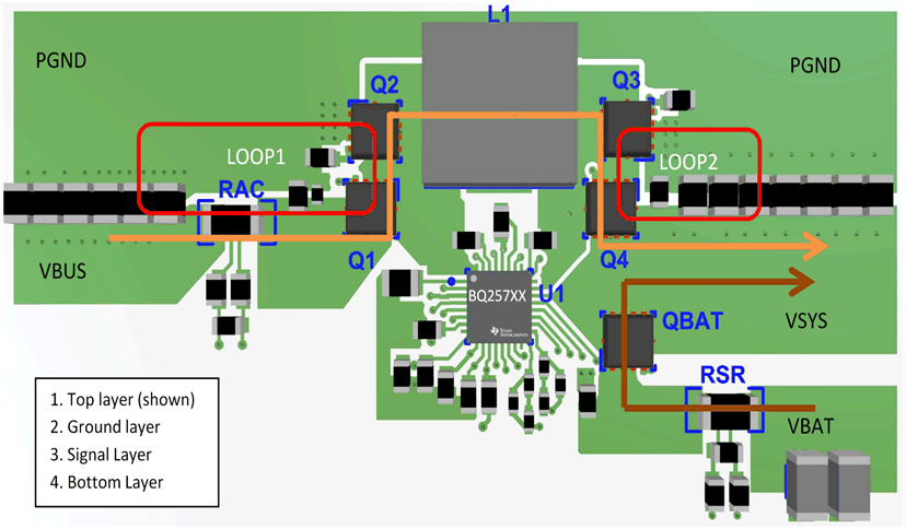
For proper layout design, multi-layer PCB is suggested. The BQ257XX EVM uses a 4-layer PCB as shown in Figure 2-1. The top layer contains power traces and most signal lines. Any remaining area on top layer must be filled with ground and be connected to bottom and internal grounds by strong via connection through all layers. The internal layer 2 is ground only and layer 3 contains signal lines and ground. The bottom layer is used for additional non-critical signals and ground.
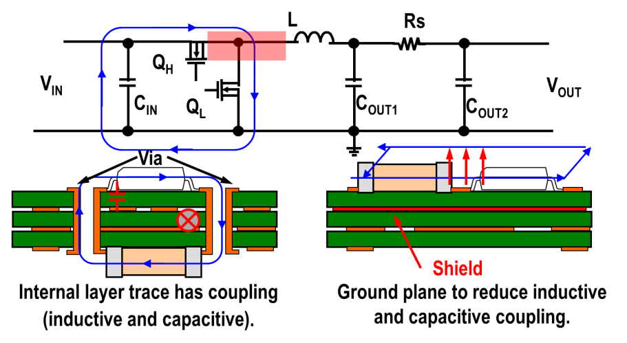
As shown in Figure 2-2, put ground near power components layer (Top layer) since that can be an effective shield to reduce inductive and capacitive coupling noise. If the ground layer is the next layer following the power stage layer, the ground layer copper gets the lowest thermal resistance, smallest high-frequency loop area and shield most of the rest circuit from the high-noise power stage. Also, if all high-current loop components are put on the same layer, the magnetic field lines are vertical to the board. So, the ground copper layer can provide the best shielding performance between the power stage circuit and other small signal circuits on the board.
 Figure 2-1 Layout Example for PCB
Stack-Up and Top Side Components Placement
 Figure 2-2 Power Stage Component
Placement and Ground Layer