SLUAAU1 January 2024 BQ25700A , BQ25708 , BQ25710 , BQ25713 , BQ25720 , BQ25723 , BQ25730 , BQ25731
- 1
- Abstract
- Trademarks
- 1Introduction
-
2Layout Guidelines
- 2.1 PCB Stack-Up (4 Layers)
- 2.2 Identifying Critical Circuit Paths
- 2.3 Input and Output Loop Placements Considering Noise, Efficiency, and Thermal Performance
- 2.4 Kelvin Sensing Circuit for Current Sense to Achieve High Accuracy
- 2.5 Small Capacitors Placements Considering Noise
- 2.6 Separating AGND and PGND
- 3References
2.3 Input and Output Loop Placements Considering Noise, Efficiency, and Thermal Performance
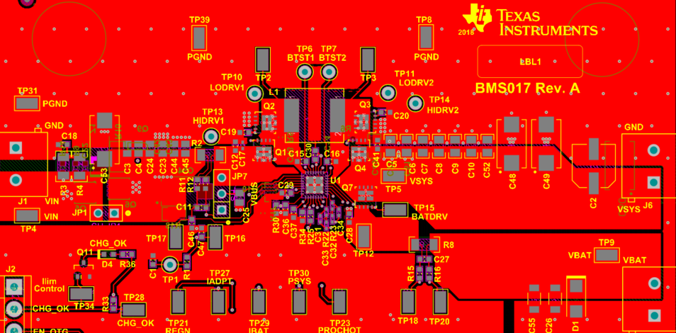
Once the critical parts of layout are identified, the next task is to minimize any sources of noise and unwanted parasitic. The input-switching current loop and output-switching current loop are the dominant high current loops. Minimize the area of these loops to suppress generated switching noise and optimize switching performance. Therefore, it’s highly recommended to put the power components on same layer. Also Allow enough copper area for thermal dissipation. Multiple thermal vias can be used to connect more copper layers together and dissipate more heat. Figure 2-4 shows the power components placement on top layer as a good example with BQ25710 EVM matching with the schematic shown in Figure 1-1.
 Figure 2-4 Power Components Placement on
Top Layer
Figure 2-4 Power Components Placement on
Top LayerVBUS capacitors, RAC, Q1 and Q2 form a small loop1. VSYS capacitors, Q3 and Q4 form a small loop 2. As shown in Figure 2-1, the most important loop areas to minimize on loop 1 and loop 2 are the path from the input capacitors through the buck high-side and low-side MOSFETs, and back to the ground connection of the input capacitor and the path from the output capacitors through the boost high-side and low-side MOSFETs, and back to the ground connection of the output capacitor. Connect the negative terminal of the capacitor close to the source of the low-side MOSFETs (at ground). Similarly, connect the positive terminal of the capacitor or capacitors close to the drain of the high-side MOSFETs of both loops. Especially 10nF + 1nF (0402 size) decoupling capacitors must be placed after RAC as close as possible to FETs for decoupling switching loop high frequency noise.
Connect the power components with large copper to reduce the parasitic resistance. Since the current path from VBUS to VSYS and VBAT to VSYS has low impedance, pay attention to via resistance if not on the same layer. The number of vias can be estimated as 1 to 2A/via for a 10mil via with 1oz copper thickness. If high density design is required, you can move part of CBUS or CSYS to the other side of PCB. Lastly, we recommend to place QBAT and RSR near the battery terminal since the device detects the battery voltage through SRN pin near battery terminal.