SLUAAU1 January 2024 BQ25700A , BQ25708 , BQ25710 , BQ25713 , BQ25720 , BQ25723 , BQ25730 , BQ25731
- 1
- Abstract
- Trademarks
- 1Introduction
-
2Layout Guidelines
- 2.1 PCB Stack-Up (4 Layers)
- 2.2 Identifying Critical Circuit Paths
- 2.3 Input and Output Loop Placements Considering Noise, Efficiency, and Thermal Performance
- 2.4 Kelvin Sensing Circuit for Current Sense to Achieve High Accuracy
- 2.5 Small Capacitors Placements Considering Noise
- 2.6 Separating AGND and PGND
- 3References
2.6 Separating AGND and PGND
Separate PGND and AGND first to avoid small signal ground coupling high current (high di/dt) ground noise. In power supply layout, separating the signal system is important, such as the feedback path which is susceptible to noise and the switching nodes that switch large current.
- AGND: a quiet ground reference for control signals (analog ground)
- PGND: a noisy ground reference for power signals (power ground)
AGND is used for all sensing, compensation, and control network ground for example: ACP/ACN/COMP1/COMP2/CMPIN/CMPOUT/IADPT/IBAT/PSYS. PGND is used as return path for power stage related large current signals.
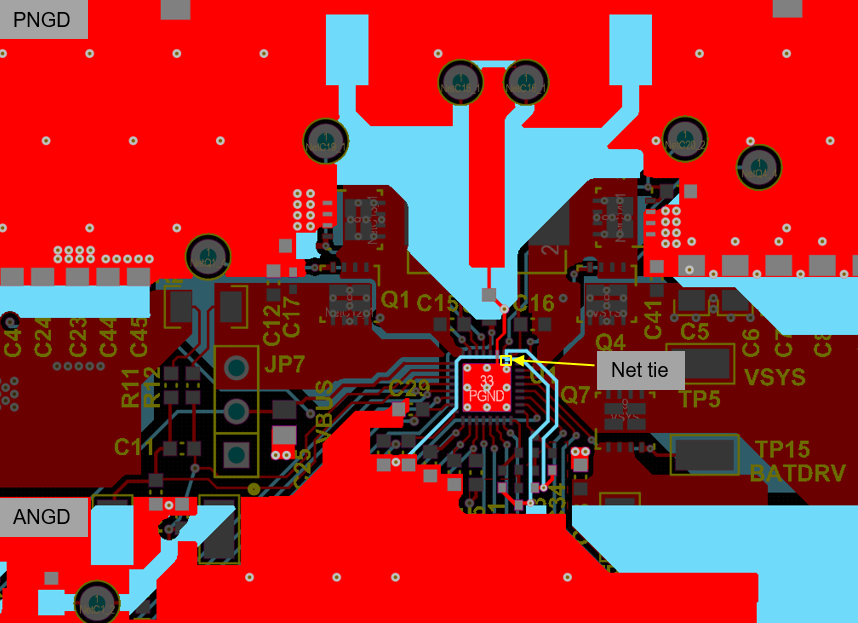
Though the DC ground potential is the same, measure must be taken to separate these AGND and PGND planes to make sure noise arising from digital or high-power signals is not conducted between them to interfere with analog signals. As shown in Figure 1-1, we recommend to have two ground signs in the schematic already as difficulties arise when visualizing sensitive and noisy potentials on the layout if the same GND sign is used on the schematic. Therefore, we recommend starting with split GND in the schematic level and connect them with a net tie (NT1).
Figure 2-8 shows the connection between PGND and AGND with a net tie in PCB layout highlighting top layer (Red) and layer3 (Blue). AGND is used for control signals and must be closer to the IC and own a polygon. Connect all AGND to a dedicated low-impedance copper lane to make sure AGND and PGND are on the same potential and ultimately must be connected together at one point near the IC as shown in Figure 2-8 (like exposed power pad underneath the IC).
 Figure 2-8 Separating AGND and PGND With
Net-Tie