SNOAA35D April 2023 – December 2023 LM2901 , LM2901B , LM2901B-Q1 , LM2903 , LM2903-Q1 , LM2903B , LM2903B-Q1 , LM339 , LM339-N , LM393 , LM393-N , LM393B , LM397 , TL331 , TL331-Q1 , TL331B
- 1
- Application Design Guidelines for LM339, LM393, TL331 Family Comparators Including the New B-versions
- Trademarks
- 1 Devices Covered in Application Note
- 2 The New TL331B, TL391B, LM339B, LM393B, LM2901B and LM2903B B Versions
-
3 Input Considerations
- 3.1 Input Stage Schematic – The Classic LM339 Family
- 3.2 Input Stage Schematic - New B Devices
- 3.3 Differences Between the Classic and B Die Devices
- 3.4 Input Voltage Range
- 3.5 Input Voltage Range vs. Common Mode Voltage Range
- 3.6 Reason for Input Range Headroom Limitation
- 3.7 Input Voltage Range Feature
- 3.8 Negative Input Voltages
- 3.9 Power-Up Behavior
- 3.10 Capacitors and Hysteresis
- 3.11 Output to Input Cross-Talk
- 4 Output Stage Considerations
- 5 Power Supply Considerations
- 6 General Comparator Usage
- 7 PSPICE and TINA TI Models
- 8 Conclusion
- 9 Related Documentation
- 10Revision History
2.2 Changes to Package Top Markings
In early 2022, TI made changes to the device top markings company-wide, and not just specific to the LM339 family. This change was covered in PCN# 20211123004 for most of the LM339 family.
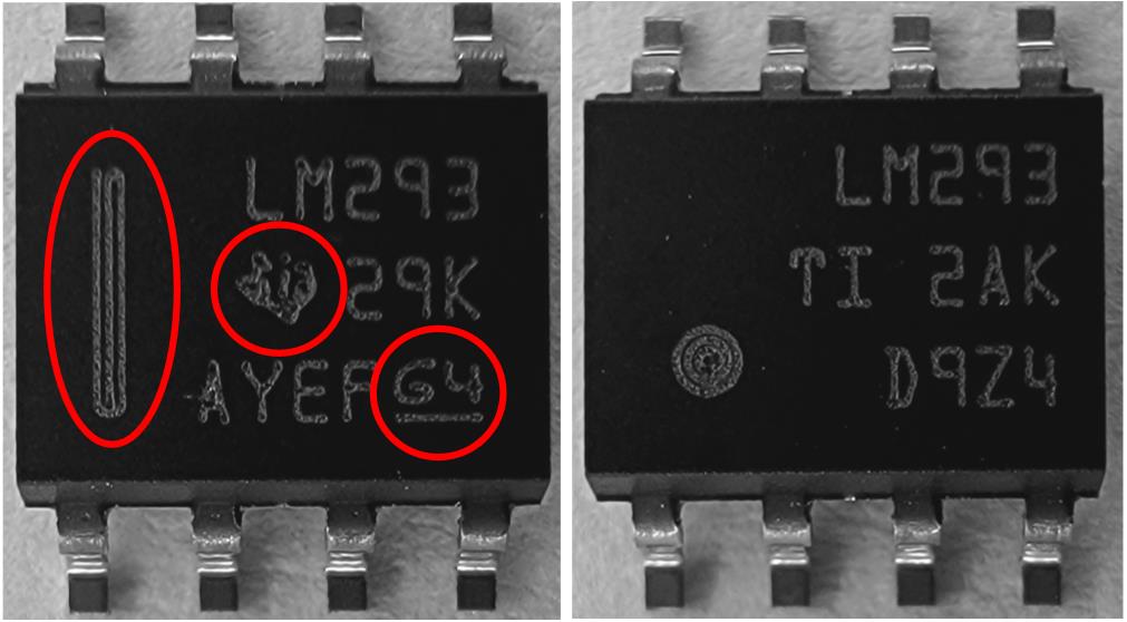
 Figure 2-3 Package Marking Change
Comparison
Figure 2-3 Package Marking Change
ComparisonThe left photo is the previous bar style marking, and the right photo is the new dot style marking.
The package marking changes are:
- The pin 1 bar marking was changed to a single dot.
- The TI logo graphic was replaced with the letters TI.
- The underscored E Category marking (commonly G4 or E4) was eliminated.
- The font was changed to a more Optical Character Recognition (OCRA) friendly font.
These label changes are gradually being applied across TI, and is possible to get a mix of the two device marking styles in large orders. The marking changes do not directly indicate which die is used, and it is still possible to get a classic die with the new top marking style.