SPRUIS4E March 2022 – January 2024
- 1
- Jacinto7 J721E/DRA829/TDA4VM Evaluation Module (EVM)
- Trademarks
- 1Introduction
- 2J721E EVM Overview
- 3EVM User Setup/Configuration
-
4J721E EVM Hardware Architecture
- 4.1 J721E EVM Hardware Top level Diagram
- 4.2 J721E EVM Interface Mapping
- 4.3 I2C Address Mapping
- 4.4 GPIO Mapping
- 4.5 Power Supply
- 4.6 Reset
- 4.7 Clock
- 4.8 Memory Interfaces
- 4.9 MCU Ethernet Interface
- 4.10 QSGMII Ethernet Interface
- 4.11 PCIe Interface
- 4.12 USB Interface
- 4.13 CAN Interface
- 4.14 FPD Interface (Audio Deserializer)
- 4.15 FPD Panel Interface (DSI Video Serializer)
- 4.16 Display Serial Interface (DSI) FPC
- 4.17 Audio Interface
- 4.18 Display Port Interface
- 4.19 MLB Interface
- 4.20 I3C Interface
- 4.21 ADC Interface
- 4.22 RTC Interface
- 4.23 Apple Authentication Header
- 4.24 EVM Expansion Connectors
- 4.25 ENET Expansion Connector
- 4.26 CSI Expansion Connector
- 5Revision History
4.11.1 X1 Lane PCIe Interface
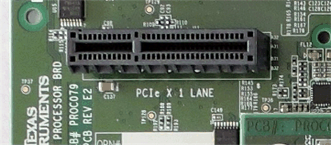
The x1 lane PCIe interface includes one x4 lane PCIe connector of part number Amphenol 10142333-10111MLF, which supports PCIe Gen4 operation. The pin-out of the connector follows PCIe standard.
The SERDES0 port of J7 SoC is connected to x1 lane PCIe socket for data transfer. PCIe0, USB0_SS and SGMII1, 2 interfaces are pinmuxed with this SERDES0 port.
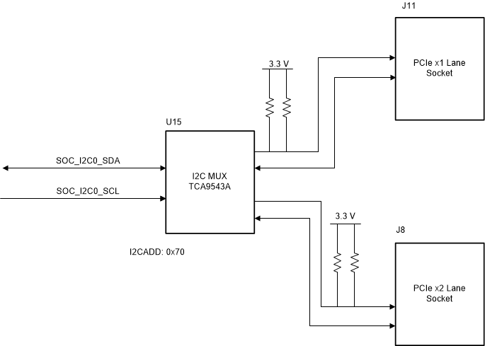
I2C0 from SoC is used for control purpose and is connected to SMBUS on the connector. I2C0 port is connected to both x1 lane and x2 lane PCIe connectors using a Mux TCA9543APWR.
 Figure 4-19 PCIe Interface for
SERDES0
 Figure 4-20 PCIe SMBUS Block
Diagram
Figure 4-20 PCIe SMBUS Block
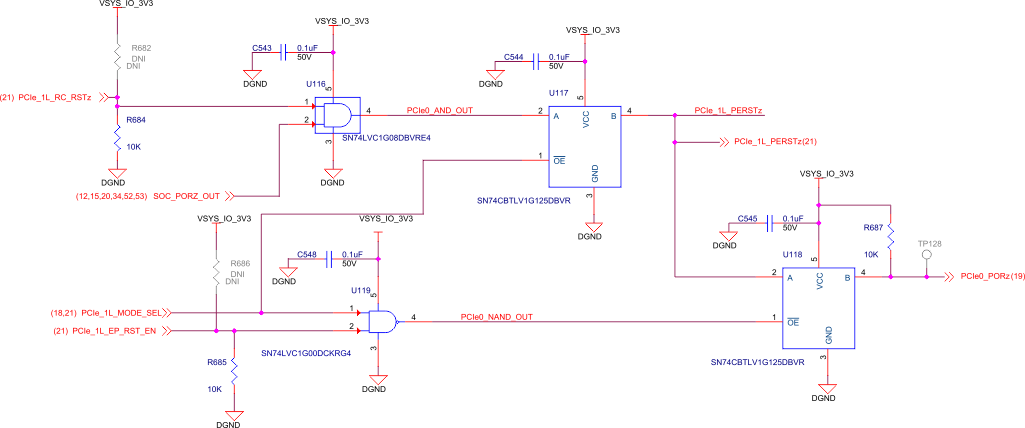
DiagramReset: A dip Switch is provided to select the reset source for host and end-point PCIe operation. In case of host mode, signal from GPIO Expander and PORz signals from SoC are ANDed and the output is connected to PCIe connector. The GPIO signal is pulled low to ensure PCIe Reset (#PERST) remains asserted until SoC releases reset.
Whereas, in case of PCIe end point operation, the CP board receives reset signal from the PCIe card.
 Figure 4-21 1L-PCIe Root Complex/Endpoint
Selection Circuit
Figure 4-21 1L-PCIe Root Complex/Endpoint
Selection CircuitClock: A clock generator (CDCI #1) is provided to drive 100 MHz HCSL clock for PCIe add on cards and SoC. Resistor options are provided to select the clock source for host and end point operation.
For PCIe host operation:
- The add on cards can have clocks driven by SOC or clock generator. Selection can be made through resistors as shown in Table 4-13.
| Clock Selected | Mount | Unmount |
|---|---|---|
| Reference Clock for SOC from clock generator | R194 | R195, C92 |
| R198 | R199, C93 | |
| Reference Clock for PCIe connector from SOC | R195, C92 | R194, R109 |
| R199, C93 | R198, R110 | |
| Reference Clock for PCIe connector from clock generator | R109 | R195, C92 |
| R110 | R199, C93 |
For PCIe Endpoint operation:
- The SOC can have the clock driven by add on cards or clock generator. Selection can be made through resistors as shown in Table 4-14.
| Clock Selected | Mount | Unmount |
|---|---|---|
| Reference clock for SOC from clock generator | R194 | R195, C92 |
| R198 | R199, C93 | |
| Reference clock for SOC from PCIe connector | R195, C92 | R194, R109 |
| R199, C93 | R198, R110 |
Hot plug: The PRSNT1# and PRSNT2# signals are the hot plug presence detect signals. The PRSNT1# is pulled up and PRSNT2# is connected to GPIO expander, so that PRSNT1# will be pulled low when a add on card is plugged in as both the PRSNT signals in add on cards will be shorted. Optional resistor is provided to short the PRSNT1# and PRSNT2# to support host and device mode.
For choosing Host or device operation of PCIe card, following resistors must be mounted/unmounted as mentioned in Table 4-15.
| Mode | Mount | Demount |
|---|---|---|
| Host mode | R674 | R675 |
| R679 | ||
| Device mode | R675 | R674 |
| R679 |
Additional Options:
Optional MDIO bus and USB2.0 interface is supported for external PCIe add on cards.
SoC Main domain (CPSW9G0) MDIO signals are interfaced to the x1L PCIe Socket (J11) through 0-Ω inline resistors (R137 and R136) when network (Ethernet) based add on cards inserted into J11. The path is disconnected by default.
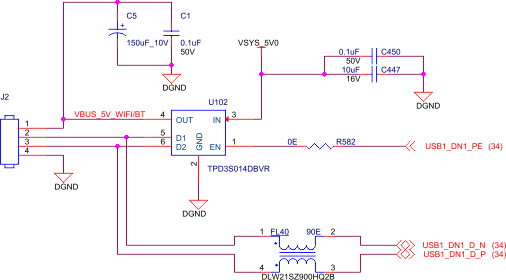
Also, USB2.0 data signals from USB HUB downstream port is interfaced to 4 pin header (J2) and the 5 V supply is provided through the load switch.
 Figure 4-22 USB2.0 Header
Connection