SPRUIS4E March   2022  – January 2024


  1.   1
  2.   Jacinto7 J721E/DRA829/TDA4VM Evaluation Module (EVM)
  3.   Trademarks
  4. 1Introduction
    1. 1.1 Key Features
    2. 1.2 Thermal Compliance
    3. 1.3 REACH Compliance
    4. 1.4 EMC, EMI, and ESD Compliance
  5. 2J721E EVM Overview
    1. 2.1 J721E EVM Board Identification
    2. 2.2 J721E SOM Component Identification
    3. 2.3 Jacinto7 Common Processor Components Identification
    4. 2.4 Quad Ethernet Components Identification
  6. 3EVM User Setup/Configuration
    1. 3.1 Power Requirements
    2. 3.2 Power ON Switch and Power LEDs
      1. 3.2.1 Over Voltage and Under Voltage Protection Circuit
      2. 3.2.2 Power Regulators and Power Status LEDs
    3. 3.3 EVM Reset/Interrupt Push Buttons
    4. 3.4 EVM DIP Switches
      1. 3.4.1 EVM Configuration DIP Switch
      2. 3.4.2 SOM Configuration DIP Switch
      3. 3.4.3 Boot Modes
      4. 3.4.4 Other Selection Switches
    5. 3.5 EVM UART/COM Port Mapping
    6. 3.6 JTAG Emulation
  7. 4J721E EVM Hardware Architecture
    1. 4.1  J721E EVM Hardware Top level Diagram
    2. 4.2  J721E EVM Interface Mapping
    3. 4.3  I2C Address Mapping
    4. 4.4  GPIO Mapping
    5. 4.5  Power Supply
      1. 4.5.1 Power Sequencing
      2. 4.5.2 Voltage Supervisor
      3. 4.5.3 DDR I/O Voltage Selection
        1. 4.5.3.1 J721E SoC S2R Logic Flow Diagram
        2. 4.5.3.2 J721E SoC MCU Only Operation
        3. 4.5.3.3 Power Monitoring
    6. 4.6  Reset
    7. 4.7  Clock
      1. 4.7.1 Processor’s Primary Clock
      2. 4.7.2 Processor’s Secondary/SERDES Ref Clock
      3. 4.7.3 EVM Peripheral Ref Clock
    8. 4.8  Memory Interfaces
      1. 4.8.1 LPDDR4 Interface
      2. 4.8.2 OSPI Interface
      3. 4.8.3 UFS Interface
      4. 4.8.4 MMC Interface
        1. 4.8.4.1 MMC0 - eMMC Interface
        2. 4.8.4.2 MMC1 – Micro SD Interface
      5. 4.8.5 Board ID EEPROM Interface
      6. 4.8.6 Boot EEPROM Interface
    9. 4.9  MCU Ethernet Interface
      1. 4.9.1 Gigabit Ethernet PHY Default Configuration
    10. 4.10 QSGMII Ethernet Interface
    11. 4.11 PCIe Interface
      1. 4.11.1 X1 Lane PCIe Interface
      2. 4.11.2 X2 Lane PCIe Interface
      3. 4.11.3 M.2 PCIe Interface
    12. 4.12 USB Interface
      1. 4.12.1 USB 3.1 Interface
      2. 4.12.2 USB 2.0 Interface
      3. 4.12.3 USB 3.0 Micro AB Interface (Reserved Port)
    13. 4.13 CAN Interface
    14. 4.14 FPD Interface (Audio Deserializer)
    15. 4.15 FPD Panel Interface (DSI Video Serializer)
    16. 4.16 Display Serial Interface (DSI) FPC
    17. 4.17 Audio Interface
    18. 4.18 Display Port Interface
    19. 4.19 MLB Interface
    20. 4.20 I3C Interface
    21. 4.21 ADC Interface
    22. 4.22 RTC Interface
    23. 4.23 Apple Authentication Header
    24. 4.24 EVM Expansion Connectors
    25. 4.25 ENET Expansion Connector
      1. 4.25.1 Power Requirements
      2. 4.25.2 Clock
        1. 4.25.2.1 Main Clock
        2. 4.25.2.2 Optional Clock
      3. 4.25.3 Reset Signals
      4. 4.25.4 Ethernet Interface
        1. 4.25.4.1 Quad Port SGMII PHY Default Configuration
      5. 4.25.5 Board ID EEPROM Interface
    26. 4.26 CSI Expansion Connector
  8. 5Revision History

MMC1 – Micro SD Interface

The EVM supports a Micro SD card interface connected to MMC1 port of SoC. The Micro SD card socket Mfr. Part# DM3BT-DSF-PEJS is interfaced with MMC1 port of SoC. This supports UHS1 operation including I/O operations at both 1.8 V and 3.3 V. The Micro SD card interface is set to operate in SD mode by default.

The I/O voltage is controlled using the LDO that provides the I/O voltage for the MMC1 port. The SD Card power is provided using a load switch, which is controlled by a GPIO from I/O expander. Control signal “GPIO_uSD_PWR_EN” is driven by the I2C I/O expander U31 Port02 on the CP board. This I/O expander is controlled by the processor’s I2C0 port. I2C address of the I/O expander is 0x22.
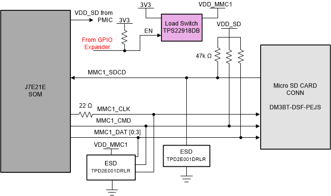
GUID-022BEB0C-26E3-4DC0-9270-9895627DE13A-low.gifFigure 4-14 micro-SD Card Block Diagram

An ESD protection device Mfr. Part# TPD2E001DRLR is provided for data, clock, command and card detect signals. The CD (card detect) pin of Micro SD card socket is pulled high and connected to CD pin of SoC. An external pull up resistor (47K) is provided on data [3:0] and CMD signals to avoid floating.