SPRUIS4E March 2022 – January 2024
- 1
- Jacinto7 J721E/DRA829/TDA4VM Evaluation Module (EVM)
- Trademarks
- 1Introduction
- 2J721E EVM Overview
- 3EVM User Setup/Configuration
-
4J721E EVM Hardware Architecture
- 4.1 J721E EVM Hardware Top level Diagram
- 4.2 J721E EVM Interface Mapping
- 4.3 I2C Address Mapping
- 4.4 GPIO Mapping
- 4.5 Power Supply
- 4.6 Reset
- 4.7 Clock
- 4.8 Memory Interfaces
- 4.9 MCU Ethernet Interface
- 4.10 QSGMII Ethernet Interface
- 4.11 PCIe Interface
- 4.12 USB Interface
- 4.13 CAN Interface
- 4.14 FPD Interface (Audio Deserializer)
- 4.15 FPD Panel Interface (DSI Video Serializer)
- 4.16 Display Serial Interface (DSI) FPC
- 4.17 Audio Interface
- 4.18 Display Port Interface
- 4.19 MLB Interface
- 4.20 I3C Interface
- 4.21 ADC Interface
- 4.22 RTC Interface
- 4.23 Apple Authentication Header
- 4.24 EVM Expansion Connectors
- 4.25 ENET Expansion Connector
- 4.26 CSI Expansion Connector
- 5Revision History
4.12.2 USB 2.0 Interface
The USB1 port of J721E SoC is used for USB 2.0 interface in J721E EVM. The USB1 signals are connected to upstream port of USB 2.0 Hub (TUSB4041IPAPR). The four downstream ports from USB Hub are connected are shown below:
- 2 USB ports are terminated to Type A Stacked Connector (AU-Y1008-2)
- 1 USB port is connected to 4 Pin Header (PCIe Card - WiFi/BT)
- 1 USB port is connected to EVM Expansion connector
The reference clock to the USB HUB is provided using 24 MHz crystal and also an optional clock input from the Peripheral clock generator using a resistor mux. The default clock source is set to crystal.
 Figure 4-28 USB Hub Reference Clock
Circuit
Figure 4-28 USB Hub Reference Clock
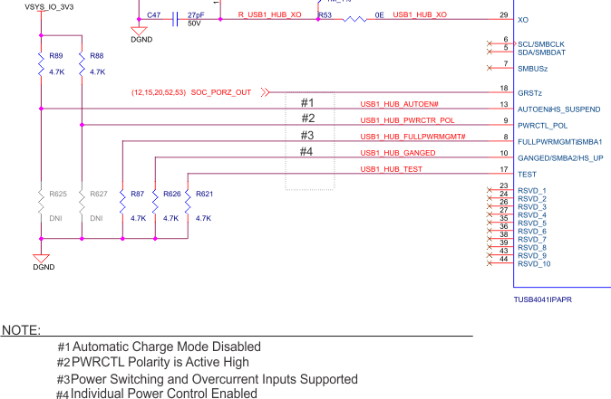
CircuitFigure 4-29 shows the USB HUB strapping options.
 Figure 4-29 USB Hub Settings
Circuit
Figure 4-29 USB Hub Settings
CircuitAnd the USB ID pin is pulled low to operate the SoC in Host mode.
 Figure 4-30 USB1 ID Setting for
HUB
Figure 4-30 USB1 ID Setting for
HUBTo PCIe Card Wi-Fi/BT:
The downstream port1 of USB HUB is connected to the Wi-Fi/BT header (J2) on the CP board. The power to the WiFi header is provided through current limit load switch with integrated ESD protection device TPD3S014DBVR. The power is controlled by USB hub power enable signal USB1_DN1_PE.
To Stacked Connector:
The downstreams port2 and 3 of USB HUB is connected to the stacked USB 2.0 Type-A receptacle AU-Y1008-2 on the CP board. The power to the USB Type-A receptacle is provided through current limit load switch with integrated ESD protection device TPD3S014DBVR for each port. The power is controlled by USB hub power enable signals USB1_DN2_PE and USB1_DN3_PE.
To Expansion Connector:
The downstream port4 of USB HUB is connected to EVM Expansion connector. The current version of EVM is not supporting any peripherals on this port. It is reserved for future development.