SPRUJ63A September 2022 – October 2023
- 1
- Trademarks
- 1Introduction
- 2Important Usage Notes
-
3System Description
- 3.1 Key Features
- 3.2 Functional Block Diagram
- 3.3 Power-On/Off Procedures
- 3.4
Peripheral and Major Component
Description
- 3.4.1 Clocking
- 3.4.2 Reset
- 3.4.3 Power
- 3.4.4 Configuration
- 3.4.5 JTAG
- 3.4.6 Test Automation
- 3.4.7 UART Interfaces
- 3.4.8 Memory Interfaces
- 3.4.9 Ethernet Interface
- 3.4.10 Display Interface
- 3.4.11 USB 2.0 Interface
- 3.4.12 PCIe Interface
- 3.4.13 High Speed Expansion Interface
- 3.4.14 CAN Interface
- 3.4.15 Interrupt
- 3.4.16 ADC Interface
- 3.4.17 Safety Connector
- 3.4.18 SPI Interfaces
- 3.4.19 I2C Interfaces
- 3.4.20 FSI Interface
- 4Known Issues and Modifications
- 5References
- 6Revision History
3.4.3.4 Power Supply
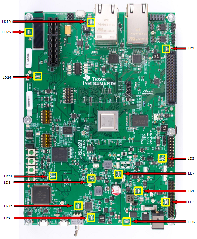
The EVM utilizes an array of DC-DC converters to supply the various memories, clocks, SoC and other components on the card with the necessary voltage and the power required. Table 3-5 gives power-good LEDs provided on EVM board to give users positive confirmation of the status of output of each supply.
Test points for each power outputs are provided on the EVM Board and are mentioned in the below Table 3-4.
Table 3-4 Power Test Points
| Sl.No | Power Supply | Test Point | Voltage |
|---|---|---|---|
| Top Side | |||
| 1 | VMAIN | TP81 | 12 V |
| 2 | VCC_5V0 | TP18 | 5 V |
| 3 | VCC3V3_PREREG | TP12 | 3.3 V |
| 4 | VCC_3V3_SYS | TP44 | 3.3 V |
| 5 | VDD_2V5 | TP6 | 2.5 V |
| 6 | VDD_1V1 | TP28 | 1.1 V |
| 7 | VDDA1V8 | TP29 | 1.8 V |
| 8 | VDD_CORE | TP14 | 0.75 V (1) |
| 9 | VCC_CORE | TP23 | 0.75 V |
| 10 | VDD_0V85 | TP8 | 0.85 V |
| 11 | VDDAR_CORE | TP10 | 0.85 V |
| 12 | VCC1V2_DDR | TP4 | 1.2 V |
| 13 | VDD_2V8 | TP99 | 2.8 V |
| 14 | VCC3V3_TA | TP96 | 3.3 V |
| 15 | VDD_1V0 | TP56 | 1 V |
| 16 | VPP_DDR_2V5 | TP47 | 2.5 V |
| 17 | VDDR_VTT | TP48 | 0.6 V |
| 18 | VCC1V8 | TP51 | 1.8 V |
| 19 | VPP_1V8 | TP52 | 1.8 V |
(1) AM243x EVM is 0.85 V.
Table 3-5 Power LEDs
| Sl.No | Power Supply | LED REF |
|---|---|---|
| Before SW1 TURN ON | ||
| 1 | VMAIN | LD6 |
| 2 | VCC3V3_TA | LD24 |
| After SW1 TURN ON | ||
| 3 | VCC_5V0 | LD15 |
| 4 | VCC3V3_PREREG | LD4 |
| 5 | VCC_3V3_SYS | LD9 |
| 6 | VDD_2V5 | LD1 |
| 7 | VDD_1V1 | LD10 |
| 8 | VDDA1V8 | LD8 |
| 9 | VDD_CORE | LD2 |
| 10 | VCC_CORE | LD7 |
| 11 | VDD_2V8 | LD25 |
| 12 | VCC1V2_DDR | LD3 |
 Figure 3-6 Power Good LEDs