SWRU548C February   2019  – September 2021 CC3235MODAS , CC3235MODASF , CC3235MODS , CC3235MODSF


  1. 1Introduction
    1. 1.1 CC3235MODSF LaunchPad™
    2. 1.2 LAUNCHCC3235MOD Key Features
    3. 1.3 What's Included
      1. 1.3.1 Kit Contents
      2. 1.3.2 Software Examples
    4. 1.4 REACH Compliance
    5. 1.5 Regulatory Compliance
    6. 1.6 First Steps: Out-of-Box Experience
      1. 1.6.1 Connecting to the Computer
      2. 1.6.2 Running the Out-of-Box Experience
    7. 1.7 Next Steps: Looking into the Provided Code
    8. 1.8 Trademarks
  2. 2Hardware
    1. 2.1 Block Diagram
    2. 2.2 Hardware Features
      1. 2.2.1  Key Benefits
      2. 2.2.2  XDS110-Based Onboard Debug Probe
      3. 2.2.3  Debug Probe Connection: Isolation Jumper Block
      4. 2.2.4  Application (or "Backchannel") UART
      5. 2.2.5  JTAG Headers
      6. 2.2.6  Using the XDS110 Debug Probe with a Different Target
      7. 2.2.7  Power Connections
        1. 2.2.7.1 XDS110 USB Power
        2. 2.2.7.2 BoosterPack Plug-in Module and External Power Supply
      8. 2.2.8  Reset Pullup Jumper
      9. 2.2.9  Clocking
      10. 2.2.10 I2C Connection
        1. 2.2.10.1 Default I2C Addresses
      11. 2.2.11 Sense on Power (SOP)
      12. 2.2.12 Push-Buttons and LED Indicators
    3. 2.3 Electrical Characteristics
    4. 2.4 Antenna Characteristics
    5. 2.5 BoosterPack Plug-in Module Pinout
  3. 3Layout Guidelines
    1. 3.1 LAUNCHCC3235MOD Board Layout
    2. 3.2 General Layout Recommendations
    3. 3.3 RF Layout Recommendations
    4. 3.4 Antenna Placement and Routing
    5. 3.5 Transmission Line Considerations
  4. 4Operational Setup and Testing
    1. 4.1 Measuring the CC3235MOD Current Draw
      1. 4.1.1 Low-Current Measurement with USB Power (<1 mA)
      2. 4.1.2 Active Current Measurements
    2. 4.2 RF Connections
      1. 4.2.1 AP Connection Testing
    3. 4.3 Design Files
      1. 4.3.1 Hardware Design Files
    4. 4.4 Software
  5. 5Development Environment Requirements
    1. 5.1 CCS
    2. 5.2 IAR
  6. 6Additional Resources
    1. 6.1 CC3235MODx Product Page
    2. 6.2 Download CCS or IAR
    3. 6.3 SimpleLink™ Academy for CC3235 SDK
    4. 6.4 TI E2E Support Forums
  7. 7Assembly Drawing and Schematics
    1. 7.1 Assembly Drawing
    2. 7.2 Schematics
      1.      A Manual Information to the End User
        1.       A.1 End User Manual
        2.       A.2 RF Function and Frequency Range
        3.       A.3 FCC and IC Certification and Statement
          1.        A.3.1 FCC
          2.        A.3.2 CAN ICES-3(B) and NMB-3(B) Certification and Statement
          3.        A.3.3 End Product Labeling
          4.        A.3.4 Device Classifications
          5.        A.3.5 FCC Definitions
          6.        A.3.6 Simultaneous Transmission Evaluation
        4.       A.4 EU Certification and Statement
          1.        A.4.1 RF Exposure Information (MPE)
          2.        A.4.2 Simplified DoC Statement
            1.         A.4.2.1 CC3235MODx and CC3235MODAx Modules
            2.         A.4.2.2 LAUNCHCC3235MOD
          3.        A.4.3 Waste Electrical and Electronic Equipment (WEEE)
          4.        A.4.4 OEM and Host Manufacturer Responsibilities
          5.        A.4.5 Antenna Specifications
        5.       A.5 CC3235MODx Approved Antennas
          1.        B Revision History

Using the XDS110 Debug Probe with a Different Target

The XDS110 debug probe on the LaunchPad development kit can interface to most Arm® Cortex®-M devices, not just the onboard target CC3235MODSF device. This functionality is enabled by the J2 10-pin Cortex-M JTAG connector (see Figure 2-8) and a 10-pin cable, such as the FFSD-05-D-06.00-01-N (sold separately from the LaunchPad development kit).
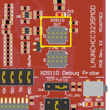
GUID-8B41D1EA-BCE1-41E4-90A7-941A09007DBE-low.pngFigure 2-8 XDS110 OUT Connector (J2)

Header J2 follows the Arm Cortex-M standard; however, pin 1 is not a voltage sense pin. The XDS110 outputs only 3.3-V JTAG signals. If another voltage level is needed, the user must provide level shifters to translate the JTAG signal voltages.

  1. Remove jumpers on the JTAG signals on the isolation block, including RST, TMS, TCK, TDO, and TDI.
  2. Plug the 10-pin cable into J2, and connect to an external target.

    J2 follows the Arm Cortex Debug Connector standard outlined in Cortex-M Debug Connectors.

  3. Plug USB power into the LaunchPad development kit, or power it externally

    JTAG levels are 3.3-V ONLY