SWRU548C February   2019  – September 2021 CC3235MODAS , CC3235MODASF , CC3235MODS , CC3235MODSF


  1. 1Introduction
    1. 1.1 CC3235MODSF LaunchPad™
    2. 1.2 LAUNCHCC3235MOD Key Features
    3. 1.3 What's Included
      1. 1.3.1 Kit Contents
      2. 1.3.2 Software Examples
    4. 1.4 REACH Compliance
    5. 1.5 Regulatory Compliance
    6. 1.6 First Steps: Out-of-Box Experience
      1. 1.6.1 Connecting to the Computer
      2. 1.6.2 Running the Out-of-Box Experience
    7. 1.7 Next Steps: Looking into the Provided Code
    8. 1.8 Trademarks
  2. 2Hardware
    1. 2.1 Block Diagram
    2. 2.2 Hardware Features
      1. 2.2.1  Key Benefits
      2. 2.2.2  XDS110-Based Onboard Debug Probe
      3. 2.2.3  Debug Probe Connection: Isolation Jumper Block
      4. 2.2.4  Application (or "Backchannel") UART
      5. 2.2.5  JTAG Headers
      6. 2.2.6  Using the XDS110 Debug Probe with a Different Target
      7. 2.2.7  Power Connections
        1. 2.2.7.1 XDS110 USB Power
        2. 2.2.7.2 BoosterPack Plug-in Module and External Power Supply
      8. 2.2.8  Reset Pullup Jumper
      9. 2.2.9  Clocking
      10. 2.2.10 I2C Connection
        1. 2.2.10.1 Default I2C Addresses
      11. 2.2.11 Sense on Power (SOP)
      12. 2.2.12 Push-Buttons and LED Indicators
    3. 2.3 Electrical Characteristics
    4. 2.4 Antenna Characteristics
    5. 2.5 BoosterPack Plug-in Module Pinout
  3. 3Layout Guidelines
    1. 3.1 LAUNCHCC3235MOD Board Layout
    2. 3.2 General Layout Recommendations
    3. 3.3 RF Layout Recommendations
    4. 3.4 Antenna Placement and Routing
    5. 3.5 Transmission Line Considerations
  4. 4Operational Setup and Testing
    1. 4.1 Measuring the CC3235MOD Current Draw
      1. 4.1.1 Low-Current Measurement with USB Power (<1 mA)
      2. 4.1.2 Active Current Measurements
    2. 4.2 RF Connections
      1. 4.2.1 AP Connection Testing
    3. 4.3 Design Files
      1. 4.3.1 Hardware Design Files
    4. 4.4 Software
  5. 5Development Environment Requirements
    1. 5.1 CCS
    2. 5.2 IAR
  6. 6Additional Resources
    1. 6.1 CC3235MODx Product Page
    2. 6.2 Download CCS or IAR
    3. 6.3 SimpleLink™ Academy for CC3235 SDK
    4. 6.4 TI E2E Support Forums
  7. 7Assembly Drawing and Schematics
    1. 7.1 Assembly Drawing
    2. 7.2 Schematics
      1.      A Manual Information to the End User
        1.       A.1 End User Manual
        2.       A.2 RF Function and Frequency Range
        3.       A.3 FCC and IC Certification and Statement
          1.        A.3.1 FCC
          2.        A.3.2 CAN ICES-3(B) and NMB-3(B) Certification and Statement
          3.        A.3.3 End Product Labeling
          4.        A.3.4 Device Classifications
          5.        A.3.5 FCC Definitions
          6.        A.3.6 Simultaneous Transmission Evaluation
        4.       A.4 EU Certification and Statement
          1.        A.4.1 RF Exposure Information (MPE)
          2.        A.4.2 Simplified DoC Statement
            1.         A.4.2.1 CC3235MODx and CC3235MODAx Modules
            2.         A.4.2.2 LAUNCHCC3235MOD
          3.        A.4.3 Waste Electrical and Electronic Equipment (WEEE)
          4.        A.4.4 OEM and Host Manufacturer Responsibilities
          5.        A.4.5 Antenna Specifications
        5.       A.5 CC3235MODx Approved Antennas
          1.        B Revision History

RF Layout Recommendations

The RF section of this wireless module gets top priority in terms of layout. It is very important for the RF section to be laid out correctly to ensure optimum performance from the module. A poor layout can cause low-output power, EVM degradation, sensitivity degradation, and mask violations.

Figure 3-5 shows the RF placement and routing of the CC3235MODSF module.
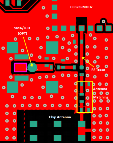
GUID-799BAEFD-0187-4ADA-93A2-81E978860F2F-low.pngFigure 3-5 RF Section Layout

Use the following RF layout recommendations for the CC3235MODx module:

  • RF traces must have 50-Ω impedance.
  • RF trace bends must be made with gradual curves, and 90 degree bends must be avoided.
  • RF traces must not have sharp corners.
  • There must be no traces or ground under the antenna section.
  • RF traces must have via stitching on the ground plane beside the RF trace on both sides.
  • RF traces must be as short as possible. The antenna, RF traces, and the module must be on the edge of the PCB product in consideration of the product enclosure material and proximity.

For optimal RF performance, ensure the copper cut out on the top layer under the RF-BG pin (pin 31) is as shown in Figure 3-6.
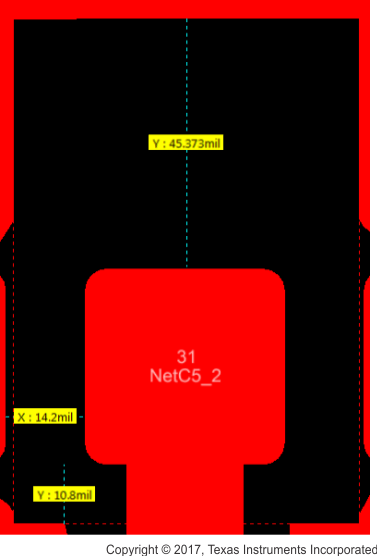
GUID-BC499895-B36E-43AC-81E4-4C4D7567476F-low.gifFigure 3-6 Top Layer Copper Pullback on RF Pads