TIDUES0E June   2019  – April 2024 TMS320F28P550SJ , TMS320F28P559SJ-Q1


  1.   1
  2.   Description
  3.   Resources
  4.   Features
  5.   Applications
  6.   6
  7. 1System Description
    1. 1.1 Key System Specifications
  8. 2System Overview
    1. 2.1 Block Diagram
    2. 2.2 Highlighted Products
      1. 2.2.1  UCC21710
      2. 2.2.2  UCC14141-Q1
      3. 2.2.3  AMC1311
      4. 2.2.4  AMC1302
      5. 2.2.5  OPA320
      6. 2.2.6  AMC1306M05
      7. 2.2.7  AMC1336
      8. 2.2.8  TMCS1133
      9. 2.2.9  TMS320F280039C
      10. 2.2.10 TLVM13620
      11. 2.2.11 ISOW1044
      12. 2.2.12 TPS2640
    3. 2.3 System Design Theory
      1. 2.3.1 Dual Active Bridge Analogy With Power Systems
      2. 2.3.2 Dual-Active Bridge – Switching Sequence
      3. 2.3.3 Dual-Active Bridge – Zero Voltage Switching (ZVS)
      4. 2.3.4 Dual-Active Bridge - Design Considerations
        1. 2.3.4.1 Leakage Inductor
        2. 2.3.4.2 Soft Switching Range
        3. 2.3.4.3 Effect of Inductance on Current
        4. 2.3.4.4 Phase Shift
        5. 2.3.4.5 Capacitor Selection
          1. 2.3.4.5.1 DC-Blocking Capacitors
        6. 2.3.4.6 Switching Frequency
        7. 2.3.4.7 Transformer Selection
        8. 2.3.4.8 SiC MOSFET Selection
      5. 2.3.5 Loss Analysis
        1. 2.3.5.1 SiC MOSFET and Diode Losses
        2. 2.3.5.2 Transformer Losses
        3. 2.3.5.3 Inductor Losses
        4. 2.3.5.4 Gate Driver Losses
        5. 2.3.5.5 Efficiency
        6. 2.3.5.6 Thermal Considerations
  9. 3Circuit Description
    1. 3.1 Power Stage
    2. 3.2 DC Voltage Sensing
      1. 3.2.1 Primary DC Voltage Sensing
      2. 3.2.2 Secondary DC Voltage Sensing
        1. 3.2.2.1 Secondary Side Battery Voltage Sensing
    3. 3.3 Current Sensing
    4. 3.4 Power Architecture
      1. 3.4.1 Auxiliary Power Supply
      2. 3.4.2 Gate Driver Bias Power Supply
      3. 3.4.3 Isolated Power Supply for Sense Circuits
    5. 3.5 Gate Driver Circuit
    6. 3.6 Additional Circuitry
    7. 3.7 Simulation
      1. 3.7.1 Setup
      2. 3.7.2 Running Simulations
  10. 4Hardware, Software, Testing Requirements, and Test Results
    1. 4.1 Required Hardware and Software
      1. 4.1.1 Hardware
      2. 4.1.2 Software
        1. 4.1.2.1 Getting Started With Software
        2. 4.1.2.2 Pin Configuration
        3. 4.1.2.3 PWM Configuration
        4. 4.1.2.4 High-Resolution Phase Shift Configuration
        5. 4.1.2.5 ADC Configuration
        6. 4.1.2.6 ISR Structure
    2. 4.2 Test Setup
    3. 4.3 PowerSUITE GUI
    4. 4.4 LABs
      1. 4.4.1 Lab 1
      2. 4.4.2 Lab 2
      3. 4.4.3 Lab 3
      4. 4.4.4 Lab 4
      5. 4.4.5 Lab 5
      6. 4.4.6 Lab 6
      7. 4.4.7 Lab 7
    5. 4.5 Test Results
      1. 4.5.1 Closed-Loop Performance
  11. 5Design Files
    1. 5.1 Schematics
    2. 5.2 Bill of Materials
    3. 5.3 Altium Project
    4. 5.4 Gerber Files
    5. 5.5 Assembly Drawings
  12. 6Related Documentation
    1. 6.1 Trademarks
  13. 7Terminology
  14. 8About the Author
  15. 9Revision History

SiC MOSFET and Diode Losses

As SiC is used in the power stage, the body diodes conduct only during the dead time, causing ZVS. In all other instances, the channel of SiC is turned on to conduct current. The peak current in the primary is calculated using Equation 7 and Equation 8. For the nominal operating conditions:

  • V1 = 800 V
  • V2 = 500 V
  • Fs= 100 kHz
  • Ts=10 μs
  • N = 1.6
  • φ = 0.4 rad
  • P = 10 kW
  • L = 35 μH

Calculating i1 and i2 for these inputs leads to i1 = i2 = 14.3 A. i1 = i2 is only true for the nominal output voltage V2 = V1 / N.

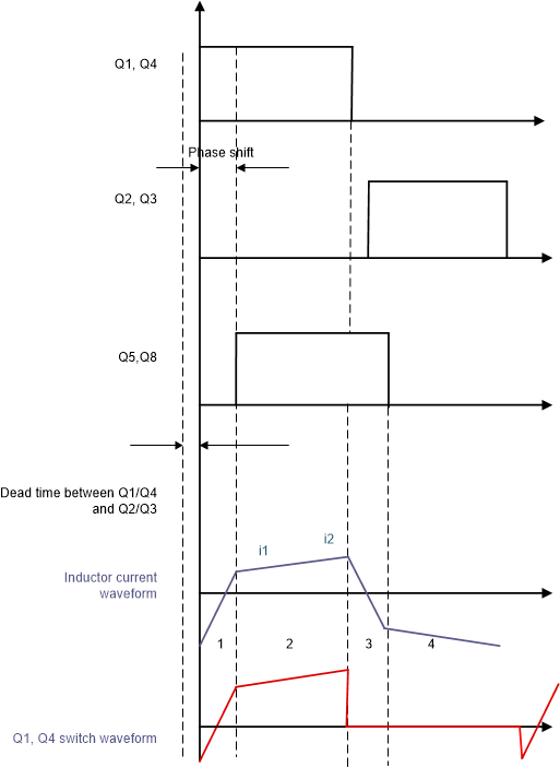
Figure 2-21 shows the current waveform of the switches on the primary side. The RMS value can be calculated from equation Equation 21. Inserting the values mentioned above leads to 9.67 A of RMS current for primary side switches.

Equation 21. I s w i t c h , p r i m , r m s = 1 6 × i 1 2 + i 2 2 + 1 - 2 φ π × i 2 × i 1 = 9.67 A

The diode conducts for only a small fraction of time during the switching period, as in the dead time causing ZVS. The dead time chosen for this application is 200 ns.

Equation 22. I d i o d e , p r i m = i 2 × t d e a d T s   = 0.286   A

The value of drain-source resistance corresponding to the applied gate voltage waveform is obtained from the SiC MOSFETs data sheet. This value is 75 mΩ. The forward voltage drop across the body diode is 5.5 V. The conduction losses across the four primary side FETs is calculated using Equation 23:

Equation 23. P c o n d , p r i m = 4 × I s w i t c h , p r i m , r m s 2 × R d s , o n + I d i o d e , p r i m × V f d , p r i m = 34.34   W

Similarly, the conduction losses are calculated across the secondary side FETs by scaling the primary side RMS currents with transformer turns ratio using Equation 24 and Equation 25. The on state resistance of the secondary side MOSFET is 30 mΩ. The forward voltage drop across the body diode is 5.5 V
Equation 24. I s w i t c h , s e c , r m s = N   × I s w i t c h , p r i m , r m s = 15.47   A
Equation 25. I d i o d e , s e c = N   × I d i o d e , p r i m = 0.458   A
Equation 26. P c o n d , s e c = 4 × I s w i t c h , s e c , r m s 2 × R d s , o n + I d i o d e , s e c × V f d , s e c = 3 7 . 88   W
TIDA-010054 Switch Current Waveforms for
                    Calculating RMS Value of Current Figure 2-21 Switch Current Waveforms for Calculating RMS Value of Current

The switching loss curves from the manufacturer are used to calculate switching losses.

Because the FETs turn on at zero voltage, only the turn-off loss coefficients are used for calculating the switching losses. Using the C3M0030090K data sheet information, a turn-off energy of 60 μJ is estimated for this operating condition. The values of switching loss per device is obtained using the information in Equation 27. This leads to 24 W of switching losses for the secondary side.

Equation 27. P s w , t u n r o f f , s e c = F s × E o f f = 6   W

For the primary side switch C3M0075120K the turn-off energy is estimated at 75 μJ. Which leads to 30 W of switching losses on the primary side.

Equation 28. P s w , t u n r o f f , p r i m = F s × E o f f = 7.5   W

Total turn off switching losses in the primary and secondary side across all eight switches comes to 54 W.

These calculations are done for the nominal operating conditions. For different operating points these calculations need to be adjusted. For non-nominal output voltages, the zero-voltage-switching can be lost and the turn-on losses must be taken into account.