SBOA511A March 2021 – September 2021 INA209 , INA219 , INA220 , INA220-Q1 , INA226 , INA226-Q1 , INA228 , INA228-Q1 , INA229 , INA229-Q1 , INA230 , INA231 , INA232 , INA233 , INA234 , INA236 , INA237 , INA237-Q1 , INA238 , INA238-Q1 , INA239 , INA239-Q1 , INA260 , INA3221 , INA3221-Q1
- Trademarks
- 1 Introduction
- 2 Defining Constraints
- 3 Find The Maximum Shunt Value
- 4 Find The Minimum Shunt Value
- 5 Maximum Resolution or Minimum Shunt Loss
- 6 What to Do if the Measurement Range Is Insufficient
- 7 Determine the Current LSB and Calibration Coefficient
- 8 Programming Your Device Registers
- 9 Summary
- 10Revision History
4 Find The Minimum Shunt Value
Upon calculating the max shunt value, the minimum shunt value should also be determined. To determine this value, you need to know the lowest meaningful shunt input voltage value. At minimum, this value corresponds to the shunt voltage register 1 LSB step size. There are some devices, like the INA209, INA219, and INA220 that for certain ADC configuration settings require a register bit higher than the LSB to be used, because the conversion time will not be sufficient to achieve the full possible resolution as alluded to in Table 4-1's test conditions column. Be sure to check the Vsense register to gain better insight into what sense values are possible and how the data is stored. Below is the Table 4-2 for the INA228. Here we can see that the lowest resolvable shunt voltage neglecting noise corresponds to 312.5nV/LSB or 78.125nV/LSB depending on a ADCRANGE setting found in another register. Also we can see the register LSB does not correspond to the lowest ADC measurement LSB, which is important to be aware of when reading from the device.
| Bit | Field | Type | Reset | Description |
|---|---|---|---|---|
| 23-4 | VSHUNT | R | 0h | Differential voltage measured across the shunt output.
Two's complement value. Conversion factor: 312.5 nV/LSB when ADCRANGE = 0 78.125 nV/LSB when ADCRANGE = 1 |
| 3-0 | RESERVED | R | 0h | Reserved. Always reads 0. |
To find the ideal RSHUNT MIN divide the shunt voltage 1 LSB step size by your minimum expected current value.
The LSB voltage corresponds the lowest measurable shunt value if error sources are neglected. The primary source of error for low current measurements is the input-referred offset voltage. This will vary with respect to common mode voltage, supply voltage, temperature, and device. As most power devices are bidirectional, you should be able to detect changes in your measured current even when the shunt voltage offset is larger than the shunt voltage LSB step size. Depending on your design, setup, and desired level of accuracy, you can calibrate this error out by taking an initial no load measurement at your common mode voltage and current conditions. If you have no intention of calibrating and are concerned about the percent error for your lower measurements, you can calculate RSHUNT MIN according to input referred offset voltage max and the percent error you can tolerate.
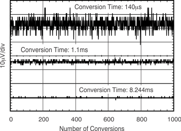
The other significant source of error particularly noticeable at your lowest measurement is noise. Your device conversion and averaging setting will determine how significantly this impacts your measurement. As can be seen from the Figure 4-1, longer conversion times lead to measurements with much less noise. With typically the longest conversion time, averaging can also be used to further reduce variability from noise.
 Figure 4-1 INA226 Noise vs. Conversion Time
| Parameter | Test Conditions | INA219A | INA219B | UNIT | |||||||
|---|---|---|---|---|---|---|---|---|---|---|---|
| MIN | TYP | MAX | MIN | TYP | MAX | ||||||
| ADC TIMING | |||||||||||
| ADC conversion time | 12 bit | 532 | 586 | 532 | 586 | µs | |||||
| 11 bit | 276 | 304 | 276 | 304 | µs | ||||||
| 10 bit | 148 | 163 | 148 | 163 | µs | ||||||
| 9 bit | 84 | 93 | 84 | 93 | µs | ||||||