SLAA530B March 2012 – July 2021 MSP430F5131 , MSP430F5132 , MSP430F5151 , MSP430F5152 , MSP430F5171 , MSP430F5172 , MSP430F5212 , MSP430F5214 , MSP430F5217 , MSP430F5219 , MSP430F5222 , MSP430F5224 , MSP430F5229 , MSP430F5232 , MSP430F5234 , MSP430F5237 , MSP430F5239 , MSP430F5242 , MSP430F5244 , MSP430F5247 , MSP430F5249 , MSP430F5252 , MSP430F5253 , MSP430F5254 , MSP430F5255 , MSP430F5256 , MSP430F5257 , MSP430F5258 , MSP430F5259 , MSP430F5304 , MSP430F5308 , MSP430F5309 , MSP430F5310 , MSP430F5324 , MSP430F5325 , MSP430F5326 , MSP430F5327 , MSP430F5328 , MSP430F5328-EP , MSP430F5329 , MSP430F5333 , MSP430F5335 , MSP430F5336 , MSP430F5338 , MSP430F5340 , MSP430F5341 , MSP430F5342 , MSP430F5358 , MSP430F5359 , MSP430F5418 , MSP430F5418A , MSP430F5419 , MSP430F5419A , MSP430F5435 , MSP430F5435A , MSP430F5436 , MSP430F5436A , MSP430F5437 , MSP430F5437A , MSP430F5438 , MSP430F5438A , MSP430F5438A-EP , MSP430F5500 , MSP430F5501 , MSP430F5502 , MSP430F5503 , MSP430F5504 , MSP430F5505 , MSP430F5506 , MSP430F5507 , MSP430F5508 , MSP430F5509 , MSP430F5510 , MSP430F5513 , MSP430F5514 , MSP430F5515 , MSP430F5517 , MSP430F5519 , MSP430F5521 , MSP430F5522 , MSP430F5524 , MSP430F5525 , MSP430F5526 , MSP430F5527 , MSP430F5528 , MSP430F5529 , MSP430F5630 , MSP430F5631 , MSP430F5632 , MSP430F5633 , MSP430F5634 , MSP430F5635 , MSP430F5636 , MSP430F5637 , MSP430F5638 , MSP430F5658 , MSP430F5659 , MSP430F6433 , MSP430F6435 , MSP430F6436 , MSP430F6438 , MSP430F6458 , MSP430F6459 , MSP430F6459-HIREL , MSP430F6630 , MSP430F6631 , MSP430F6632 , MSP430F6633 , MSP430F6634 , MSP430F6635 , MSP430F6636 , MSP430F6637 , MSP430F6638 , MSP430F6658 , MSP430F6659 , MSP430F6720 , MSP430F6720A , MSP430F6721 , MSP430F6721A , MSP430F6723 , MSP430F6723A , MSP430F6724 , MSP430F6724A , MSP430F6725 , MSP430F6725A , MSP430F6726 , MSP430F6726A , MSP430F6730 , MSP430F6730A , MSP430F6731 , MSP430F6731A , MSP430F6733 , MSP430F6733A , MSP430F6734 , MSP430F6734A , MSP430F6735 , MSP430F6735A , MSP430F6736 , MSP430F6736A , MSP430F6745 , MSP430F67451 , MSP430F67451A , MSP430F6745A , MSP430F6746 , MSP430F67461 , MSP430F67461A , MSP430F6746A , MSP430F6747 , MSP430F67471 , MSP430F67471A , MSP430F6747A , MSP430F6748 , MSP430F67481 , MSP430F67481A , MSP430F6748A , MSP430F6749 , MSP430F67491 , MSP430F67491A , MSP430F6749A , MSP430F67621 , MSP430F67621A , MSP430F67641 , MSP430F67641A , MSP430F6765 , MSP430F67651 , MSP430F67651A , MSP430F6765A , MSP430F6766 , MSP430F67661 , MSP430F67661A , MSP430F6766A , MSP430F6767 , MSP430F67671 , MSP430F67671A , MSP430F6767A , MSP430F6768 , MSP430F67681 , MSP430F67681A , MSP430F6768A , MSP430F6769 , MSP430F67691 , MSP430F67691A , MSP430F6769A , MSP430F6775 , MSP430F67751 , MSP430F67751A , MSP430F6775A , MSP430F6776 , MSP430F67761 , MSP430F67761A , MSP430F6776A , MSP430F6777 , MSP430F67771 , MSP430F67771A , MSP430F6777A , MSP430F6778 , MSP430F67781 , MSP430F67781A , MSP430F6778A , MSP430F6779 , MSP430F67791 , MSP430F67791A , MSP430F6779A , MSP430FR2000 , MSP430FR2032 , MSP430FR2033 , MSP430FR2100 , MSP430FR2110 , MSP430FR2111 , MSP430FR2153 , MSP430FR2155 , MSP430FR2310 , MSP430FR2311 , MSP430FR2353 , MSP430FR2355 , MSP430FR2422 , MSP430FR2433 , MSP430FR2475 , MSP430FR2476 , MSP430FR2512 , MSP430FR2522 , MSP430FR2532 , MSP430FR2533 , MSP430FR2632 , MSP430FR2633 , MSP430FR2672 , MSP430FR2673 , MSP430FR2675 , MSP430FR2676 , MSP430FR4131 , MSP430FR4132 , MSP430FR4133 , MSP430FR5041 , MSP430FR5043 , MSP430FR50431 , MSP430FR5720 , MSP430FR5721 , MSP430FR5722 , MSP430FR5723 , MSP430FR5724 , MSP430FR5725 , MSP430FR5726 , MSP430FR5727 , MSP430FR5728 , MSP430FR5729 , MSP430FR5730 , MSP430FR5731 , MSP430FR5732 , MSP430FR5733 , MSP430FR5734 , MSP430FR5735 , MSP430FR5736 , MSP430FR5737 , MSP430FR5738 , MSP430FR5739 , MSP430FR5739-EP , MSP430FR5847 , MSP430FR58471 , MSP430FR5848 , MSP430FR5849 , MSP430FR5857 , MSP430FR5858 , MSP430FR5859 , MSP430FR5867 , MSP430FR58671 , MSP430FR5868 , MSP430FR5869 , MSP430FR5870 , MSP430FR5872 , MSP430FR58721 , MSP430FR5887 , MSP430FR5888 , MSP430FR5889 , MSP430FR58891 , MSP430FR5922 , MSP430FR59221 , MSP430FR5947 , MSP430FR59471 , MSP430FR5948 , MSP430FR5949 , MSP430FR5957 , MSP430FR5958 , MSP430FR5959 , MSP430FR5962 , MSP430FR5964 , MSP430FR5967 , MSP430FR5968 , MSP430FR5969 , MSP430FR5969-SP , MSP430FR59691 , MSP430FR5970 , MSP430FR5972 , MSP430FR59721 , MSP430FR5986 , MSP430FR5987 , MSP430FR5988 , MSP430FR5989 , MSP430FR5989-EP , MSP430FR59891 , MSP430FR5992 , MSP430FR5994 , MSP430FR59941 , MSP430FR6005 , MSP430FR6007 , MSP430FR6035 , MSP430FR6037 , MSP430FR60371 , MSP430FR6041 , MSP430FR6043 , MSP430FR60431 , MSP430FR6045 , MSP430FR6047 , MSP430FR60471 , MSP430FR6820 , MSP430FR6822 , MSP430FR68221 , MSP430FR6870 , MSP430FR6872 , MSP430FR68721 , MSP430FR6877 , MSP430FR6879 , MSP430FR68791 , MSP430FR6887 , MSP430FR6888 , MSP430FR6889 , MSP430FR68891 , MSP430FR6920 , MSP430FR6922 , MSP430FR69221 , MSP430FR6927 , MSP430FR69271 , MSP430FR6928 , MSP430FR6970 , MSP430FR6972 , MSP430FR69721 , MSP430FR6977 , MSP430FR6979 , MSP430FR69791 , MSP430FR6987 , MSP430FR6988 , MSP430FR6989 , MSP430FR69891
- Trademarks
- 1Introduction to ESD
- 2General System-Level ESD Design Guidelines
- 3System Efficient ESD Design (SEED)
- 4SEED-Based IEC Protection Design and Verification – Real World Example 1
- 5System-Level ESD Protection – Real World Example 2
- 6Summary
- 7Modeling Using TLP Parameters
- 8References
- Revision History
4.4 Isolated Impedance Calculation
Figure 4-3 shows the SEED method simulation of the IEC protection using SEED parameters to model the TVS device and the MSP430 I/O pin as discussed in previous sections.
 Figure 4-3 SEED Method Simulation Schematic
Figure 4-3 shows that the IEC ESD current pulse is first bypassed to GND by the TVS device (primary clamp) and the decoupling capacitor; thus, limiting the induced voltage of the IEC stress pulse. The TVS max diode breakdown voltage plus the dynamic voltage across the TVS (based on the on-resistance and current through the TVS) represents the voltage of the residual pulse that is presented at the isolation impedance. Using a decoupling capacitor in parallel to the TVS model limits the voltage due to the initial fast transient current peak of the IEC pulse at the TVS node. Therefore, for all further calculations, the peak IEC current of the slow discharge curve (which is approximately 18 A) is used. With max IEC pulse current (IIEC,max) approximately 18 A and TVS on-resistance (RTVS,on,max) approximately 1 Ω, the maximum voltage of the residual pulse presented at the isolated impedance is calculated as:
VTVS,max = VTVS,t1,max + (IIEC,max × RTVS,on,max)
VTVS,max = 9.5 V + (18 A × 1 Ω)
VTVS,max ≈ 27.5 V
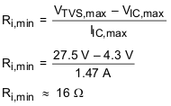
In this case, the isolation impedance is represented by a resistor between the primary and secondary clamps. The value of this resistor is calculated based on the max voltage drop across the resistor required such that the worst-case ESD current and voltage presented at the IC pin is not violated by the residual ESD stress
Given the MSP430 I/O pin on-chip ESD protection turn-on voltage (when ESD protection is triggered) of VIC,t1,min = 2.6 V, minimum on-resistance value of RIC,on,min = 1.15 Ω, and the maximum acceptable current of IIC,max = 1.47 A, the maximum acceptable voltage that can be presented to the IC pin is calculated as:
VIC,max = VIC,t1,min + (IIC,max × RIC,on,min)
VIC,max = 2.6 V + (1.47 A × 1.15 Ω)
VIC,max ≈ 4.3 V
As a result, the minimum isolation or decoupling resistance value is calculated as: