SNAA320B November 2019 – January 2024 LM4040-N , LM4050-N , LM4128 , LM4128-Q1 , LM4132 , LM4132-Q1 , REF102 , REF1925 , REF1930 , REF1933 , REF1941 , REF20-Q1 , REF200 , REF2025 , REF2030 , REF2033 , REF2041 , REF2125 , REF2912 , REF2920 , REF2925 , REF2930 , REF2933 , REF2940 , REF3012 , REF3020 , REF3025 , REF3030 , REF3033 , REF3033-Q1 , REF31-Q1 , REF3112 , REF3120 , REF3125 , REF3130 , REF3133 , REF3140 , REF3212 , REF3212-EP , REF3220 , REF3220-EP , REF3225 , REF3225-EP , REF3230 , REF3230-EP , REF3233 , REF3240 , REF3312 , REF3318 , REF3320 , REF3325 , REF3330 , REF3333 , REF34-Q1 , REF3425 , REF3425-EP , REF3430 , REF3430-EP , REF3433 , REF3433-EP , REF3440 , REF3440-EP , REF3450 , REF35 , REF4132 , REF4132-Q1 , REF5010 , REF5020 , REF5020-EP , REF5020A-Q1 , REF5025 , REF5025-EP , REF5025-HT , REF5025A-Q1 , REF5030 , REF5030A-Q1 , REF5040 , REF5040-EP , REF5040A-Q1 , REF5045 , REF5045A-Q1 , REF5050 , REF5050-EP , REF5050A-Q1 , REF54 , REF6125 , REF6133 , REF6141 , REF6145 , REF6150 , REF6225 , REF6230 , REF6233 , REF6241 , REF6245 , REF6250 , REF70 , TL431LI , TL432LI , TLV431
7 Dynamic Error (Voltage Reference Driving Capability)
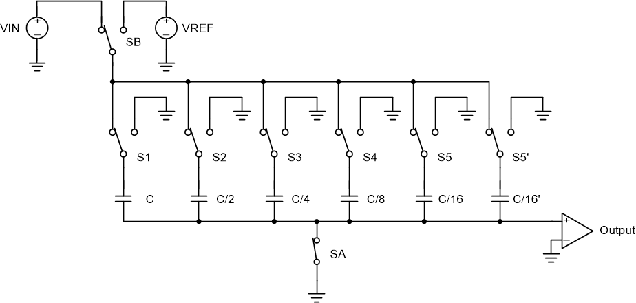
SAR ADC logic first samples input before starting digital conversion. After that, SAR ADC samples VREF at appropriate cap for every bit conversion. Hence a charge re-distribution takes place on every bit conversion on reference pin of the ADC. The magnitude of peak current is proportional to the clock frequency of the data converter. MSB conversion requires maximum charge at the cap and LSB requires minimum charge. Hence current varies from MSB to LSB conversion. This current variation changes the output according to the output impedance. This variation gets translated into non- linear error.
 Figure 7-1 SAR ADC Sampling
Architecture
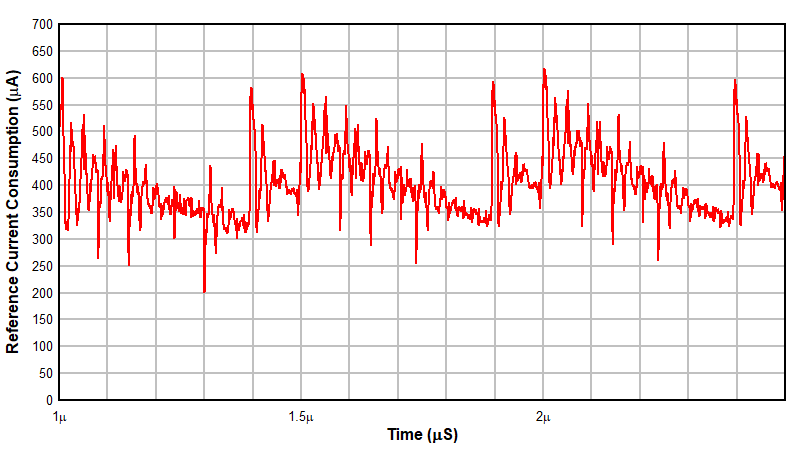
 Figure 7-2 SAR ADC VREF Current
Consumption
Figure 7-2 SAR ADC VREF Current
ConsumptionFigure 7-2 shows plot for transient current at 12 bit TI SAR AD7049 at AVDD (Reference pin) for 1V input when REF3433-Q1 is used as reference and sampling (CS) frequency is 2MHz and 64MHz Clock frequency. The load cap at reference pin is 10µF. The current is measured by measuring drop across 500Ω placed between reference pin of ADC and REF3433Q.
Time period for each conversion is 0.5µs. The data conversion takes place from 3rd clock to 14th clock from MSB to LSB (which is first half of one cycle){reference – ADC data sheet}.Each clock during the conversion is giving current spike due to charge redistribution. We can see that current spike is nonlinear varying from MSB to LSB. Max current taken by reference pin SAR ADC during conversion is 600µA for 1V input. This current varies with input magnitude. This leads to a nonlinear variation in the output of the reference device which introduces harmonic distortion in the ADC output as the Voltage-reference impact on total harmonic distortion white paper shows.
To increase switching load driving capability, a capacitor must be placed very near to reference pin of SAR ADC. Stability of the reference must also be considered while selecting the cap.
If the current demand is very high (in case a reference is driving more than one ADC), a low noise buffer at the output can be used.
The other care about is the trace resistance from output pin of shunt reference to the reference pin of ADC. Max voltage drop across trace must be much less than LSB/2 . Voltage drop across the trace is equal to Rtrace × Imax. This directly gets added to the load regulation error. One needs to also minimize trace lengths to reduce the trace inductance. To minimize this error the reference must be placed very close to the VREF pin of the ADC. If the reference has VOUT sense pin then problem of trace resistance can be eliminated by connecting output sense pin to reference pin of ADC.