SPRACM9B June   2019  – November 2020 TMS320F28384D , TMS320F28384S , TMS320F28386D , TMS320F28386S , TMS320F28388D , TMS320F28388S , TMS320F28P650DH , TMS320F28P650DK , TMS320F28P650SH , TMS320F28P650SK , TMS320F28P659DH-Q1 , TMS320F28P659DK-Q1 , TMS320F28P659SH-Q1


  1.   Trademarks
  2. Introduction
    1. 1.1 Acronyms Used in This Document
  3. Benefits of the TMS320F2838x MCU for High-Bandwidth Current Loop
  4. Current Loops in Servo Drives
  5. Outline of the Fast Current Loop Library
  6. Fast Current Loop Evaluation
    1. 5.1 Evaluation Setup
      1. 5.1.1 Hardware
      2. 5.1.2 Software
      3. 5.1.3 FCL With T-Format Type Position Encoder
        1. 5.1.3.1 Connecting T-Format Encoder to IDDK
        2. 5.1.3.2 T-Format Interface Software
        3. 5.1.3.3 T-Format Encoder Latency Considerations
      4. 5.1.4 SDFM
      5. 5.1.5 Incremental System Build
  7. Incremental Build Level 1
    1. 6.1 SVGEN Test
    2. 6.2 Testing SVGEN With DACs
    3. 6.3 Inverter Functionality Verification
  8. Incremental Build Level 2
    1. 7.1 Setting the Overcurrent Limit in the Software
    2. 7.2 Current Sense Method
    3. 7.3 Voltage Sense Method
    4. 7.4 Setting Current Regulator Limits
    5. 7.5 Verification of Current Sense
    6. 7.6 Position Encoder Feedback
      1. 7.6.1 Speed Observer and Position Estimator
      2. 7.6.2 Verification of Position Encoder Orientation
  9. Incremental Build Level 3
    1. 8.1 Observation One – PWM Update Latency
      1. 8.1.1 From the Expressions Window
      2. 8.1.2 From the Scope Plot
  10. Incremental Build Level 4
    1. 9.1 Observation
  11. 10Incremental Build Level 5
  12. 11Incremental Build Level 6
    1. 11.1 Integrating SFRA Library
    2. 11.2 Initial Setup Before Starting SFRA
    3. 11.3 SFRA GUIs
    4. 11.4 Setting Up the GUIs to Connect to Target Platform
    5. 11.5 Running the SFRA GUIs
    6. 11.6 Influence of Current Feedback SNR
    7. 11.7 Inferences
      1. 11.7.1 Bandwidth Determination From Closed Loop Plot
      2. 11.7.2 Phase Margin Determination From Open Loop Plot
      3. 11.7.3 Maximum Modulation Index Determination From PWM Update Time
      4. 11.7.4 Voltage Decoupling in Current Loop
    8. 11.8 Phase Margin vs Gain Crossover Frequency
  13. 12Incremental Build Level 7
    1. 12.1 Run the Code on CPU1 to Allocate ECAT to CM
    2. 12.2 Run the Code on CM to Setup ECAT
    3. 12.3 Setup TwinCAT
    4. 12.4 Scanning for EtherCAT Devices via TwinCAT
    5. 12.5 Program ControlCard EEPROM for ESC
    6. 12.6 Running the Application
  14. 13Incremental Build Level 8
    1. 13.1 Run the Code on CPU1 to Allocate ECAT to CM
    2. 13.2 Run the Code on CM to Setup ECAT
    3. 13.3 Running the Application
  15. 14References
  16. 15Revision History

From the Scope Plot

Note:

Because H7 is not populated, GPIO16 and GPIO18 are used for timing purposes instead of for designed functional assignment. If H7 is to become populated, comment out the associated code and restore the functional assignment.

Figure 8-3 shows the latency discussed previously in the form of a scope plot, where the rising edge of the channel 2 and channel 1 waveforms signify the instances of the ADC SoC event and completion of all PWM updates, respectively. These events are brought out over GPIO16 and GPIO18, and may be probed over [Main]-R31 and [Main]-R33, respectively. The time seen in the scope plot may be slightly more than fclLatencyInMicroSec. This additional time is needed for the CPU to return from FCL library and to set GPIO .
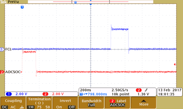
GUID-4A7D190E-BE8D-458F-97AF-5FAB24A094B4-low.gifFigure 8-3 Scope Plot of ADCSoC and FCL Completion Events