TIDUET7G September 2019 – October 2023
- 1
- Description
- Resources
- Features
- Applications
- 6
- 1System Description
-
2System Overview
- 2.1 Block Diagram
- 2.2 Design Considerations
- 2.3
Highlighted Products
- 2.3.1 LMG3422R050 — 600-V GaN With Integrated Driver and Protection
- 2.3.2 TMCS1100 — Precision Isolated Current Sense Monitor
- 2.3.3 UCC27524 — Dual, 5-A, High-Speed Low-Side Power MOSFET Driver
- 2.3.4 UCC27714 — 620-V, 1.8-A, 2.8-A High-Side Low-Side Gate Driver
- 2.3.5 ISO7721 — High Speed, Robust EMC, Reinforced and Basic Dual-Channel Digital Isolator
- 2.3.6 ISO7740 and ISO7720 — High-Speed, Low-Power, Robust EMC Digital Isolators
- 2.3.7 OPA237 — Single-Supply Operational Amplifier
- 2.3.8 INAx180 — Low- and High-Side Voltage Output, Current-Sense Amplifiers
- 2.3.9 TPS560430 — SIMPLE SWITCHER 4-V to 36-V, 600-mA Synchronous Step-Down Converter
- 2.3.10 TLV713 — 150-mA Low-Dropout (LDO) Regulator With Foldback Current Limit for Portable Devices
- 2.3.11 TMP61 — Small Silicon-Based Linear Thermistor for Temperature Sensing
- 2.3.12 CSD18510Q5B — 40-V, N-Channel NexFET MOSFET, Single SON5x6, 0.96 mOhm
- 2.3.13 UCC28911 — 700-V Flyback Switcher With Constant-Voltage, Constant-Current, and Primary-Side Regulation
- 2.3.14 SN74LVC1G3157DRYR — Single-Pole Double-Throw Analog Switch
- 2.4
System Design Theory
- 2.4.1 Totem Pole PFC Stage Design
- 2.4.2
Design Parameters of the LLC Stage
- 2.4.2.1 Determining LLC Transformer Turns Ratio N
- 2.4.2.2 Determining Mg_min and Mg_max
- 2.4.2.3 Determining Equivalent Load Resistance (Re) of Resonant Network
- 2.4.2.4 Selecting Lm and Lr Ratio (Ln) and Qe
- 2.4.2.5 Determining Primary-Side Currents
- 2.4.2.6 Determining Secondary-Side Currents
- 2.4.2.7 Primary-Side GaN and Driver
- 2.4.2.8 Secondary-Side Synchronous MOSFETs
- 2.4.2.9 Output Current Sensing
- 2.4.3 Communication Between the Primary Side and the Secondary Side
-
3Hardware, Software, Testing Requirements, and Test Results
- 3.1
Required Hardware and Software
- 3.1.1 Hardware
- 3.1.2
PFC Stage Software
- 3.1.2.1 Opening Project Inside CCS
- 3.1.2.2 Project Structure
- 3.1.2.3 Using CLA on C2000 MCU to Alleviate CPU Burden
- 3.1.2.4 CPU Utilization and Memory Allocation
- 3.1.2.5 Running the Project
- 3.1.3 LLC Stage Software
- 3.1.4 PFC + LLC Stage Dual Test
- 3.1.5 Live Firmware Update Overview
- 3.2 Testing and Results
- 3.1
Required Hardware and Software
- 4Design Files
- 5Software Files
- 6Related Documentation
- 7About the Author
- 8Revision History
- 132
3.1.3.5.2.4 Run the Code
- Run the code by using the <F8> key or the Run button (
 ) on the toolbar.
 - Use a load of 10 A at the 12-V output.
- Set the 380-V DC supply. Set the power supply current limit to an appropriate level for this test. Next, turn ON this 380-V power supply.
- At this point the output voltage should still be zero as the converter Start command has not been initiated.
- Now set the LLC_startFlag to 1 in the Expressions Window.
- The converter operation should start and the output should ramp-up to approximately 12 V.Note: If the output voltage does not ramp up to approximately 12 V, turn OFF the 380-V DC supply immediately. Verify lab 1 operation first as described in Section 3.1.3.5.1. The user may also be required to re-verify the board components and debug hardware issues (components do not match the bill of materials (BOM), PCB fabrication issue, and so forth) before this board can be tested again.
- Observe the effect of varying load on the output voltage and input current. There should be virtually no effect on the output voltage. Similarly, observe the effect of varying the input voltage. Again there should be virtually no effect on the output voltage.
- Different waveforms, like the PWM gate drive signals, input voltage, and current and output voltage may also be probed using an oscilloscope. Appropriate safety precautions should be taken and appropriate grounding requirements should be considered while probing these high voltages and high currents for this isolated DC/DC converter.
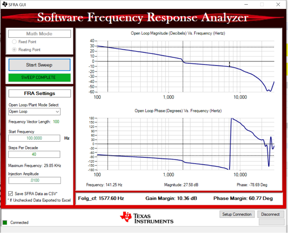
- Select the main.syscfg file and open SFRA. Click on setup connection, and select the appropriate COM port. Make sure that the baud rate is set to 57600 and that Boot on Connect is unchecked. Click the OK button. Select Floating Point math. Click Connect on the SFRA GUI. Once the GUI is connected, click on Start Sweep. SFRA will start applying different frequencies and collecting the response for frequency analysis.
 Figure 3-30 SFRA Run, LLC Closed Loop, Open Loop Gain
 - Turn OFF the 380-V DC power supply.
- Fully halting the MCU when in real-time mode is a two-step process. First halt the processor by using the Halt button on the toolbar (
 ) or by using Target → Halt. Then take the MCU out of real-time mode by clicking on
  . Finally, reset the MCU by clicking on
  .
. - Close CCS debug session by clicking on Terminate Debug Session (Target → Terminate all)
 .
.