TIDUET7G September 2019 – October 2023
- 1
- Description
- Resources
- Features
- Applications
- 6
- 1System Description
-
2System Overview
- 2.1 Block Diagram
- 2.2 Design Considerations
- 2.3
Highlighted Products
- 2.3.1 LMG3422R050 — 600-V GaN With Integrated Driver and Protection
- 2.3.2 TMCS1100 — Precision Isolated Current Sense Monitor
- 2.3.3 UCC27524 — Dual, 5-A, High-Speed Low-Side Power MOSFET Driver
- 2.3.4 UCC27714 — 620-V, 1.8-A, 2.8-A High-Side Low-Side Gate Driver
- 2.3.5 ISO7721 — High Speed, Robust EMC, Reinforced and Basic Dual-Channel Digital Isolator
- 2.3.6 ISO7740 and ISO7720 — High-Speed, Low-Power, Robust EMC Digital Isolators
- 2.3.7 OPA237 — Single-Supply Operational Amplifier
- 2.3.8 INAx180 — Low- and High-Side Voltage Output, Current-Sense Amplifiers
- 2.3.9 TPS560430 — SIMPLE SWITCHER 4-V to 36-V, 600-mA Synchronous Step-Down Converter
- 2.3.10 TLV713 — 150-mA Low-Dropout (LDO) Regulator With Foldback Current Limit for Portable Devices
- 2.3.11 TMP61 — Small Silicon-Based Linear Thermistor for Temperature Sensing
- 2.3.12 CSD18510Q5B — 40-V, N-Channel NexFET MOSFET, Single SON5x6, 0.96 mOhm
- 2.3.13 UCC28911 — 700-V Flyback Switcher With Constant-Voltage, Constant-Current, and Primary-Side Regulation
- 2.3.14 SN74LVC1G3157DRYR — Single-Pole Double-Throw Analog Switch
- 2.4
System Design Theory
- 2.4.1 Totem Pole PFC Stage Design
- 2.4.2
Design Parameters of the LLC Stage
- 2.4.2.1 Determining LLC Transformer Turns Ratio N
- 2.4.2.2 Determining Mg_min and Mg_max
- 2.4.2.3 Determining Equivalent Load Resistance (Re) of Resonant Network
- 2.4.2.4 Selecting Lm and Lr Ratio (Ln) and Qe
- 2.4.2.5 Determining Primary-Side Currents
- 2.4.2.6 Determining Secondary-Side Currents
- 2.4.2.7 Primary-Side GaN and Driver
- 2.4.2.8 Secondary-Side Synchronous MOSFETs
- 2.4.2.9 Output Current Sensing
- 2.4.3 Communication Between the Primary Side and the Secondary Side
-
3Hardware, Software, Testing Requirements, and Test Results
- 3.1
Required Hardware and Software
- 3.1.1 Hardware
- 3.1.2
PFC Stage Software
- 3.1.2.1 Opening Project Inside CCS
- 3.1.2.2 Project Structure
- 3.1.2.3 Using CLA on C2000 MCU to Alleviate CPU Burden
- 3.1.2.4 CPU Utilization and Memory Allocation
- 3.1.2.5 Running the Project
- 3.1.3 LLC Stage Software
- 3.1.4 PFC + LLC Stage Dual Test
- 3.1.5 Live Firmware Update Overview
- 3.2 Testing and Results
- 3.1
Required Hardware and Software
- 4Design Files
- 5Software Files
- 6Related Documentation
- 7About the Author
- 8Revision History
- 132
3.1.2.5.4.3 Running Code
- The project is programmed to wait for input voltage to excel at approximately 75 VRMS to drive the inrush relay, and clear the trip.
- Run the project by clicking on
 .
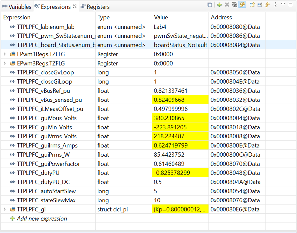
. - Now apply an input voltage of approximately 220 V. The board comes out of the undervoltage condition and inrush relay is driven. The trip clears, and the output rises to 380-V DC. A sinusoidal current is drawn from the AC input. Figure 3-19 shows the watch window when the program is running at this stage.
 Figure 3-19 PFC Lab 4: Expressions View After AC Voltage is Applied
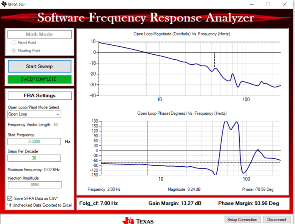
 - SFRA is integrated in the software of this build to verify the designed compensator provides enough gain and phase margin by measuring on hardware. To run the SFRA, keep the project running, and from the syscfg page, click on the SFRA icon. SFRA GUI appears.
- Select the options for the device on the SFRA GUI. For example, for F28004x, select floating point. Click on Setup Connection, and on the pop-up window, uncheck the boot on connect option and select an appropriate COM port. Click OK. Return to the SFRA GUI, and click Connect.
- The SFRA GUI connects to the device. A SFRA sweep can now be started by clicking Start Sweep. The complete SFRA sweep takes a few minutes to finish. Activity can be monitored by seeing the progress bar on the SFRA GUI and checking the flashing of blue LED on the back on the control card that indicates UART activity. Once complete, a graph with the open loop plot appears, as seen in Figure 3-20. This action verifies that the designed compensator is indeed stable. The frequency response data is also saved in the project folder under an SFRA data folder and is time stamped with the time of the SFRA run.
 Figure 3-20 SFRA Run on PFC Closed Voltage Loop
 - This verifies the voltage compensator design.
- To bring the system to a safe stop, switch off the output from the AC power supply thus bring the input AC voltage down to zero, observe the TTPLPFC_guiVbus_Volts comes down to zero as well.
- Fully halting the MCU when in real-time mode is a two-step process. First halt the processor by using the Halt button on the toolbar (
 ) or by using Target → Halt. Then take the MCU out of real-time mode by clicking on
  . Finally, reset the MCU by clicking on
  .
.10. Close CCS debug session by clicking on Terminate Debug Session (Target → Terminate all)
 .
.