TIDUET7G September 2019 – October 2023
- 1
- Description
- Resources
- Features
- Applications
- 6
- 1System Description
-
2System Overview
- 2.1 Block Diagram
- 2.2 Design Considerations
- 2.3
Highlighted Products
- 2.3.1 LMG3422R050 — 600-V GaN With Integrated Driver and Protection
- 2.3.2 TMCS1100 — Precision Isolated Current Sense Monitor
- 2.3.3 UCC27524 — Dual, 5-A, High-Speed Low-Side Power MOSFET Driver
- 2.3.4 UCC27714 — 620-V, 1.8-A, 2.8-A High-Side Low-Side Gate Driver
- 2.3.5 ISO7721 — High Speed, Robust EMC, Reinforced and Basic Dual-Channel Digital Isolator
- 2.3.6 ISO7740 and ISO7720 — High-Speed, Low-Power, Robust EMC Digital Isolators
- 2.3.7 OPA237 — Single-Supply Operational Amplifier
- 2.3.8 INAx180 — Low- and High-Side Voltage Output, Current-Sense Amplifiers
- 2.3.9 TPS560430 — SIMPLE SWITCHER 4-V to 36-V, 600-mA Synchronous Step-Down Converter
- 2.3.10 TLV713 — 150-mA Low-Dropout (LDO) Regulator With Foldback Current Limit for Portable Devices
- 2.3.11 TMP61 — Small Silicon-Based Linear Thermistor for Temperature Sensing
- 2.3.12 CSD18510Q5B — 40-V, N-Channel NexFET MOSFET, Single SON5x6, 0.96 mOhm
- 2.3.13 UCC28911 — 700-V Flyback Switcher With Constant-Voltage, Constant-Current, and Primary-Side Regulation
- 2.3.14 SN74LVC1G3157DRYR — Single-Pole Double-Throw Analog Switch
- 2.4
System Design Theory
- 2.4.1 Totem Pole PFC Stage Design
- 2.4.2
Design Parameters of the LLC Stage
- 2.4.2.1 Determining LLC Transformer Turns Ratio N
- 2.4.2.2 Determining Mg_min and Mg_max
- 2.4.2.3 Determining Equivalent Load Resistance (Re) of Resonant Network
- 2.4.2.4 Selecting Lm and Lr Ratio (Ln) and Qe
- 2.4.2.5 Determining Primary-Side Currents
- 2.4.2.6 Determining Secondary-Side Currents
- 2.4.2.7 Primary-Side GaN and Driver
- 2.4.2.8 Secondary-Side Synchronous MOSFETs
- 2.4.2.9 Output Current Sensing
- 2.4.3 Communication Between the Primary Side and the Secondary Side
-
3Hardware, Software, Testing Requirements, and Test Results
- 3.1
Required Hardware and Software
- 3.1.1 Hardware
- 3.1.2
PFC Stage Software
- 3.1.2.1 Opening Project Inside CCS
- 3.1.2.2 Project Structure
- 3.1.2.3 Using CLA on C2000 MCU to Alleviate CPU Burden
- 3.1.2.4 CPU Utilization and Memory Allocation
- 3.1.2.5 Running the Project
- 3.1.3 LLC Stage Software
- 3.1.4 PFC + LLC Stage Dual Test
- 3.1.5 Live Firmware Update Overview
- 3.2 Testing and Results
- 3.1
Required Hardware and Software
- 4Design Files
- 5Software Files
- 6Related Documentation
- 7About the Author
- 8Revision History
- 132
3.1.2.2 Project Structure
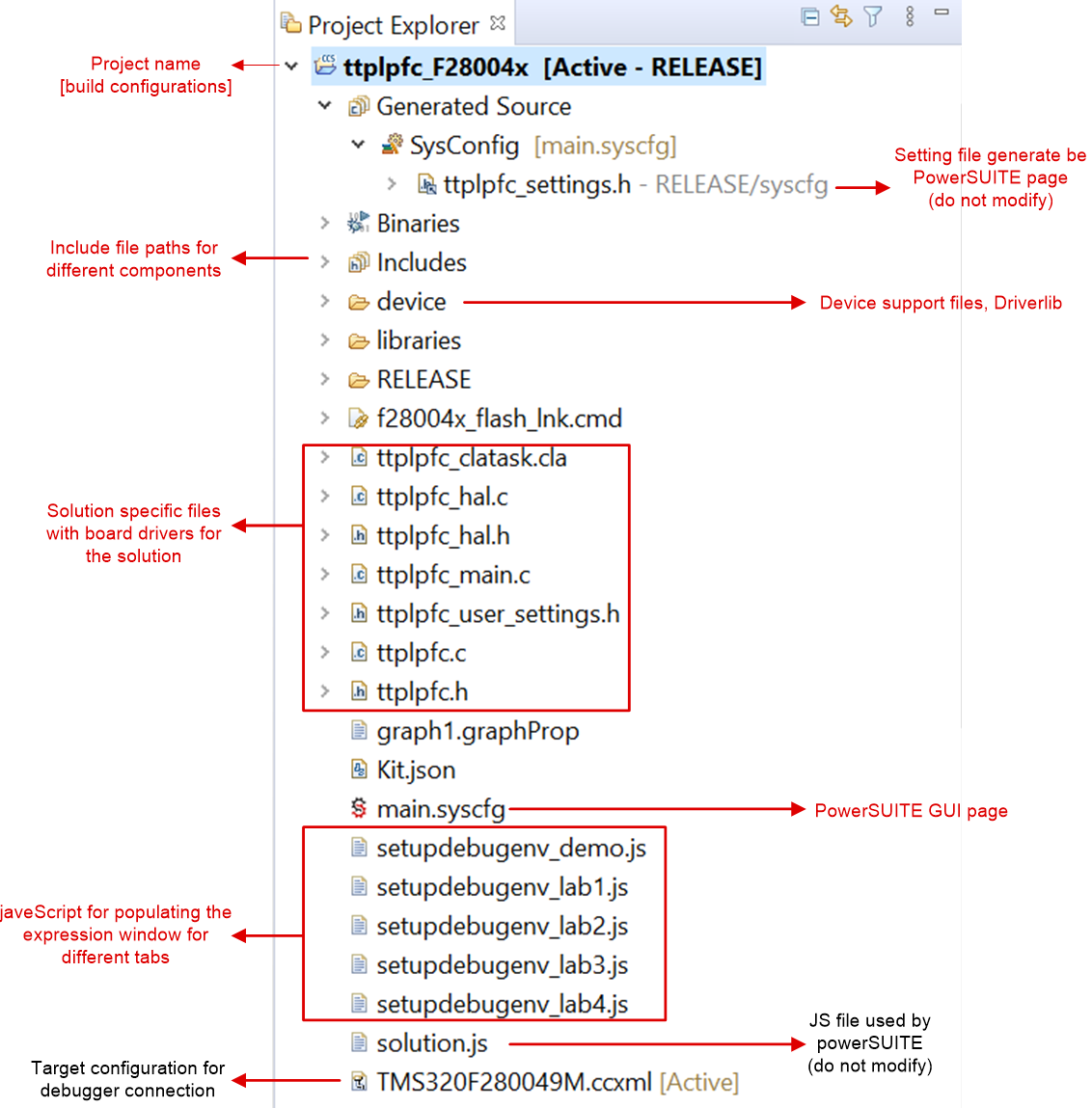
Once the project is imported, the project explorer appears inside CCS as shown in Figure 3-2.

Figure 3-2 Project Explorer View of PFC Solution Project
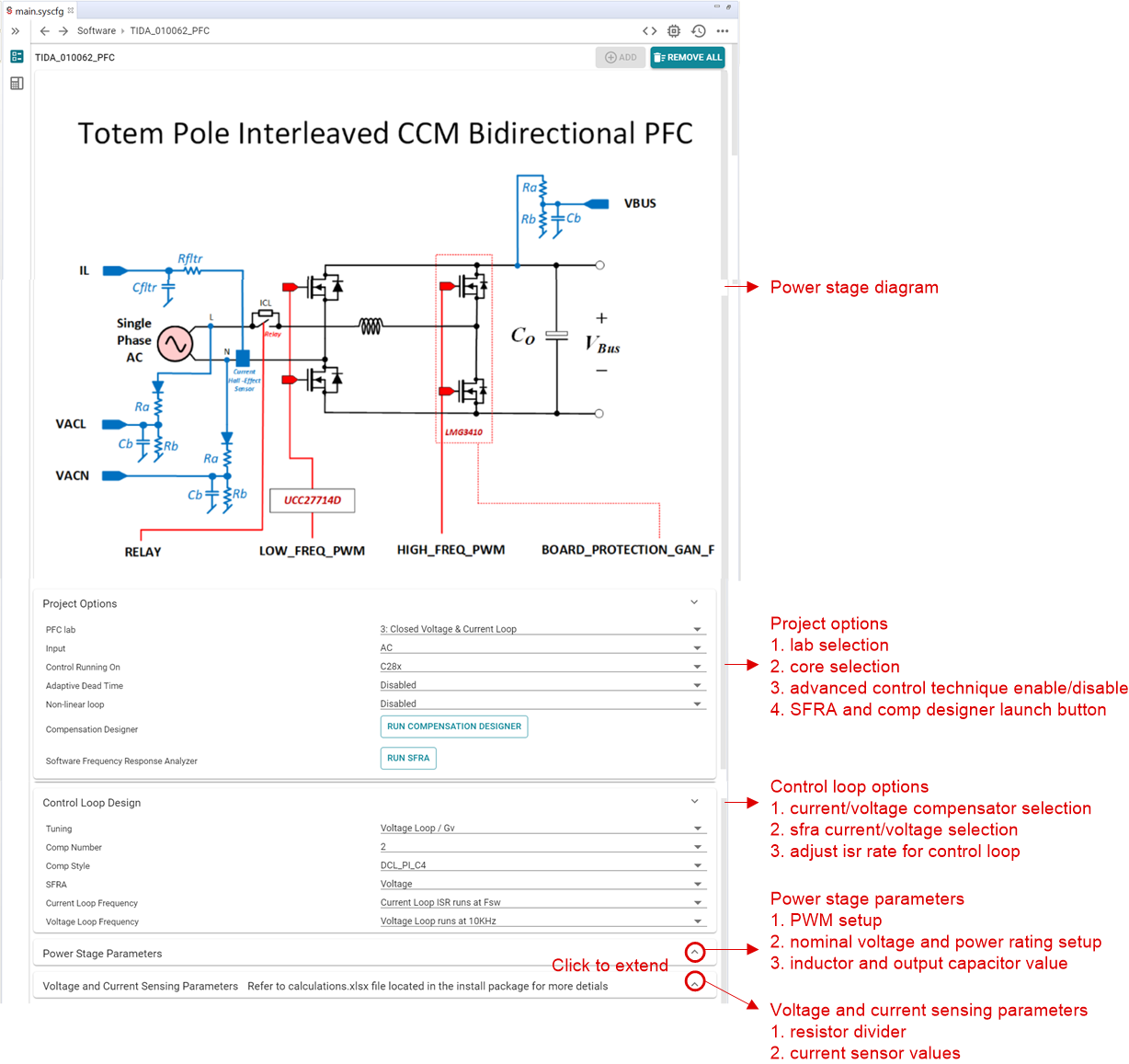
Click main.syscfg file, a GUI page appears with modifiable options for the PFC solution (Figure 3-3). This GUI can be used to change the parameters for an adapted solution, like power rating, inductance, capacitance, sensing circuit parameters, and so forth.

Figure 3-3 powerSUITE Page for CCM TTPL PFC Stage
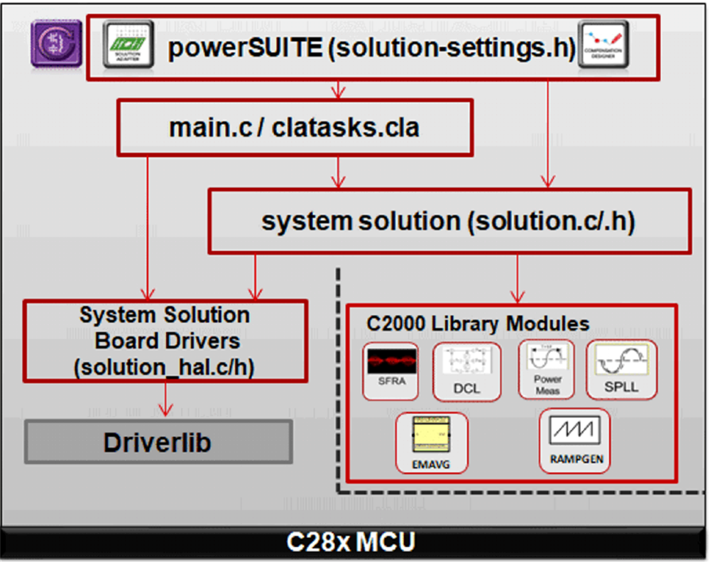
The general structure of the project is shown in Figure 3-4.

Figure 3-4 Project Structure Overview
Figure 3-4 shows the project for F28004x/F28002x/F28003x; however, if a different device is chosen from the powerSUITE page, the structure is similar.
Solution specific and device independent files are <solution>.c/h. This file consists of the main.c file of the project and is responsible for the control structure of the solution.
For this stage of this design <solution> is ttplpfc.
Board-specific and device-specific files are <solution>_hal.c/h. This file consists of device specific drivers to run the solution.
The powerSUITE page can be opened by clicking on the main.syscfg file, listed under the project explorer. The powerSUITE page generates the <solution>_settings.h file. This file is the only file used in the compile of the project that is generated by the powerSUITE page. The user must not modify this file manually as the changes are overwritten by powerSUITE every time the project is saved. User can modify several settings in <solution>_user_settings.h file.
The Kit.json and solution.js files are used internally by the powerSUITE and must also not be modified by the user. Any changes to these files result in project not functioning properly.
The setupdebugenv_build.js are provided to auto-populate the watch window variables for different labs.
The *.graphProp files is provided to auto populate settings for the data logger graph.
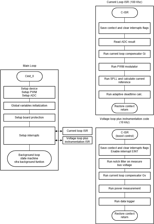
The project consists of an interrupt service routine, which is called every PWM cycle, and a current controller is run inside this ISR. In addition to this, there is a slower ISR of approximately 10 kHz that is called for running the voltage loop and the instrumentation ISR. A few background tasks (A0-A4 and B0-B4) are called in a polling fashion and can be used to run slow tasks for which absolute timing accuracy is not required, such as SFRA background and so on.
Figure 3-5 shows the software flow diagram of the firmware.
 Figure 3-5 PFC Stage Software Structure
To simplify the system, bring up and design the software of this reference design is organized in 4 labs. The lab1 and lab2 are designed to validate Boost DC-DC operation. The lab3 and lab4 are designed to validate PFC AC-DC operation.
Lab 1: Open Loop, DC (PFC Mode)
Lab 3: Closed Current Loop, AC (PFC)
Lab 4: Closed Voltage and Current Loop (PFC)
These labs are detailed in Section 3.1.2.5. If using the reference design hardware, make sure the hardware setup is completed as outlined in Section 3.1.1.