SNAS425C October 2007 – October 2014 LM98519
PRODUCTION DATA.
- 1 Features
- 2 Applications
- 3 Description
- 4 Revision History
- 5 Pin Configuration and Functions
- 6 Specifications
-
7 Detailed Description
- 7.1 Overview
- 7.2 Functional Block Diagrams
- 7.3 Feature Description
- 7.4 Device Functional Modes
- 7.5 Programming
- 7.6 Register Maps
- 8 Application and Implementation
- 9 Power Supply Recommendations
- 10Layout
- 11Device and Documentation Support
- 12Mechanical, Packaging, and Orderable Information
Package Options
Mechanical Data (Package|Pins)
- PFC|80
Thermal pad, mechanical data (Package|Pins)
Orderable Information
1 Features
- 3.3-V Single Supply Operation
- CDS or S/H Processing with Negative Input Signal Polarity
- 32.5-MHz Channel Rate
- Enhanced ESD Protection on Host Interface Pins: SHP, SHD, CLPIN, BLKCLP, AGC_ONB, MCLK, RESETB, SENB, SCLK, SDI, SDO
- Low Power CMOS Design
- 4-Wire Serial interface
- 2 Channel Symmetrical Architecture
- Independent Gain and Offset Correction for Each Channel
- Digital Black Level Calibration for Each Channel
- Digital White Level Calibration for Each Channel
- Programmable Input Clamp
2 Applications
- Digital Color Copiers
- Scanners
- Image Processing Polarity applications
-
Key Specifications
- Maximum Input Level:
- 1.19 Vp-p (CDS Gain = 1.0)
- 0.58 Vp-p (CDS Gain = 2.1)
- Input Sample Rate:
- 5 to 32.5 MSPS – 6ch Mode
- 10 to 32.5 MSPS – 3ch Mode
- PGA Gain Range: 1x to 10x (0 to 20 dB)
- CDS/SH Gain Settings: 1x or 2.1x
- Total Channel Gain: 1x to 20x (0 to 26 dB)
- PGA Gain Resolution: 8 Bits – Analog
- ADC Resolution: 10 Bits
- ADC Sampling Rate: 10 to 65 MSPS
- SNR: 67.5 dB (Gain = 1x)
- Offset DAC Range:
- ±111 mV or ±60 mV – FDAC
- ±277 mV – CDAC
- Offset DAC Resolution:
- ±10 Bits – FDAC
- ±4 Bits – CDAC
- Supply Voltage: 3.0 V to 3.6 V
- Power Dissipation: 1.04 W (Typical)
- Maximum Input Level:
3 Description
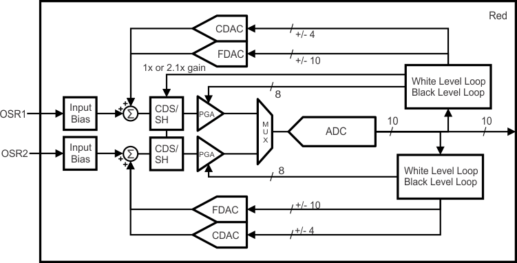
The LM98519 is a fully integrated, high performance 10-Bit, 65 MSPS signal processing solution for digital color copiers, scanners, and other image processing applications. High-speed signal throughput is achieved with an innovative six channel architecture utilizing Correlated Double Sampling (CDS), or Sample and Hold (SH) type sampling. 1x or 2x gain settings are available in the CDS/SH input stage. Each channel has a dedicated 1x to 10x (8 bit) PGA that allows accurate gain adjustment of each channel. The Digital White Level auto calibration loop can automatically set the PGA value to achieve a selected white target level. Each channel also has a ±4-bit coarse and ±10-bit fine analog offset correction DAC that allows offset correction before the sample-and-hold amplifier. These correction values can be controlled by an automated Digital Black Level correction loop. The PGA and offset DACs for each channel are programmed independently allowing unique values of gain and offset for each of the six channels. A 2-to-1 multiplexing scheme routes the signals to three 65-MHz high performance ADCs. The fully differential processing channels achieve exceptional noise immunity, having a very low noise floor of -67.5 dB. The 10-bit analog-to-digital converters have excellent dynamic performance making the LM98519 transparent in the image reproduction chain.
Device Information(1)
| PART NUMBER | PACKAGE | BODY SIZE (NOM) |
|---|---|---|
| LM98519 | TQFP (80) | 12.00 mm × 12.00 mm |
- For all available packages, see the orderable addendum at the end of the datasheet.
Simplified Schematic
4 Revision History
Changes from B Revision (April 2013) to C Revision
- Added, updated, or revised the following sections: Device Information Table, Application and Implementation; Power Supply Recommendations; Layout; Device and Documentation Support; Mechanical, Packaging, and Ordering InformationGo
- Changed 68 db to 67.5 db in Description section.Go
Changes from A Revision (April 2013) to B Revision
- Changed layout of National data sheet to TI formatGo