SLLS236I October 1996 – June 2015 SN65LBC184 , SN75LBC184
PRODUCTION DATA.
- 1 Features
- 2 Applications
- 3 Description
- 4 Revision History
- 5 Pin Configuration and Functions
-
6 Specifications
- 6.1 Absolute Maximum Ratings
- 6.2 ESD Ratings
- 6.3 Recommended Operating Conditions
- 6.4 Thermal Information
- 6.5 Electrical Characteristics: Driver
- 6.6 Electrical Characteristics: Receiver
- 6.7 Driver Switching Characteristics
- 6.8 Receiver Switching Characteristics
- 6.9 Dissipation Ratings
- 6.10 Typical Characteristics
- 7 Parameter Measurement Information
- 8 Detailed Description
- 9 Application and Implementation
- 10Power Supply Recommendations
- 11Layout
- 12Device and Documentation Support
- 13Mechanical, Packaging, and Orderable Information
Package Options
Mechanical Data (Package|Pins)
Thermal pad, mechanical data (Package|Pins)
Orderable Information
1 Features
- Integrated Transient Voltage Suppression
- ESD Protection for Bus Terminals Exceeds:
±30 kV IEC 61000-4-2, Contact Discharge
±15 kV IEC 61000-4-2, Air-Gap Discharge
±15 kV EIA/JEDEC Human Body Model - Circuit Damage Protection of 400-W Peak (Typical) Per IEC 61000-4-5
- Controlled Driver Output-Voltage Slew Rates Allow Longer Cable Stub Lengths
- 250-kbps in Electrically Noisy Environments
- Open-Circuit Fail-Safe Receiver Design
- 1/4 Unit Load Allows for 128 Devices Connected on Bus
- Thermal Shutdown Protection
- Power-Up and Power-Down Glitch Protection
- Each Transceiver Meets or Exceeds the Requirements of TIA/EIA-485 (RS-485) and ISO/IEC 8482:1993(E) Standards
- Low Disabled Supply Current 300 μA Maximum
- Pin Compatible With SN75176
2 Applications
- Industrial Networks
- Utility Meters
- Motor Control
3 Description
The SN75LBC184 and SN65LBC184 devices are differential data line transceivers in the trade-standard footprint of the SN75176 with built-in protection against high-energy noise transients. This feature provides a substantial increase in reliability for better immunity to noise transients coupled to the data cable over most existing devices. Use of these circuits provides a reliable low-cost direct-coupled (with no isolation transformer) data line interface without requiring any external components.
The SN75LBC184 and SN65LBC184 can withstand overvoltage transients of 400-W peak (typical). The conventional combination wave called out in IEC 61000-4-5 simulates the overvoltage transient and models a unidirectional surge caused by overvoltages from switching and secondary lightning transients.
Device Information(1)
| PART NUMBER | PACKAGE | BODY SIZE (NOM) |
|---|---|---|
| SN65LBC184, SN75LBC184 |
SOIC (8) | 4.90 mm × 3.91 mm |
| PDIP (8) | 9.81 mm × 6.35 mm |
- For all available packages, see the orderable addendum at the end of the datasheet.
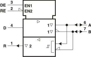
Logic Symbol

NOTE:
This symbol is in accordance with ANSI/IEEE Std 91-1984 and IEC Publication 617-12.